SNVS549C June 2009 – February 2016 LM3554
PRODUCTION DATA.
- 1 Features
- 2 Applications
- 3 Description
- 4 Revision History
- 5 Specifications
-
6 Detailed Description
- 6.1 Overview
- 6.2 Functional Block Diagram
- 6.3
Feature Description
- 6.3.1 Start-Up
- 6.3.2 Overvoltage Protection
- 6.3.3 Current Limit
- 6.3.4 Flash Termination (Strobe-Initiated Flash)
- 6.3.5 Flash Termination (I2C-Initiated Flash)
- 6.3.6 Flash Timeout
- 6.3.7 Torch Mode
- 6.3.8 TX1/Torch
- 6.3.9 ENVM/TX2/GPIO2
- 6.3.10 Indicator LED/Thermistor (LEDI/NTC)
- 6.3.11 Alternative External Torch (AET Mode)
- 6.3.12 Input Voltage Monitor
- 6.3.13 LM3554 Timing Diagrams
- 6.3.14 Flags Register and Fault Indicators
- 6.3.15 Thermal Shutdown
- 6.3.16 LED Fault
- 6.3.17 Flash Timeout
- 6.3.18 LED Thermal Fault
- 6.3.19 Input Voltage Monitor Fault
- 6.3.20 TX1 And TX2 Interrupt Flags
- 6.3.21 Light Load Disable
- 6.4 Device Functional Modes
- 6.5 Programming
- 6.6 Register Maps
-
7 Application and Implementation
- 7.1 Application Information
- 7.2
Typical Application
- 7.2.1 Design Requirements
- 7.2.2 Detailed Design Procedure
- 7.2.3 Application Curves
- 8 Power Supply Recommendations
- 9 Layout
- 10Device and Documentation Support
- 11Mechanical, Packaging, and Orderable Information
Package Options
Mechanical Data (Package|Pins)
- YFQ|16
Thermal pad, mechanical data (Package|Pins)
Orderable Information
1 Features
- Input Voltage: 2.5 V to 5.5 V
- Programmable 4.5-V or 5-V Constant Output Voltage
- Dual High-Side Current Sources
- Grounded Cathode Allowing for Better Heat Sinking and LED Routing
- > 90% Efficiency
- Ultra-Small Solution Size: < 23 mm2
- Four Operating Modes: Torch, Flash, LED Indicator, and Voltage Output
- Accurate and Programmable LED Current from 37.5 mA to 1.2 A
- Hardware Flash and Torch Enable
- LED Thermal Sensing and Current Scaleback
- Software Selectable Input Voltage Monitor
- Programmable Flash Timeout
- Dual Synchronization Inputs for RF Power-Amplifier Pulse Events
- Open and Short LED Detection
- Active High Hardware Enable for Protection Against System Faults
- 400-kHz I2C-Compatible Interface
2 Applications
- Camera Phone LED Flash Controller
- Class D Audio Amplifier Power
- LED Current Source Biasing
3 Description
The LM3554 is a 2-MHz fixed-frequency, current-mode synchronous boost converter. The device is designed to operate as a dual 600-mA (1.2 A total) constant-current driver for high-current white LEDs, or as a regulated 4.5-V or 5-V voltage source.
The main features include: an I2C-compatible interface for controlling the LED current or the desired output voltage, a hardware flash enable input for direct triggering of the flash pulse, and dual TX inputs which force the flash pulse into a low-current torch mode allowing for synchronization to RF power amplifier events or other high-current conditions. Additionally, an active high hardware enable (HWEN) input provides a hardware shutdown during system software failures.
Five protection features are available within the LM3554 including a software selectable input voltage monitor, an internal comparator for interfacing with an external temperature sensor, four selectable current limits to ensure the battery current is kept below a predetermined peak level, an overvoltage protection feature to limit the output voltage during LED open circuits, and an output short circuit protection which limits the output current during shorts to GND.
Device Information(1)
| PART NUMBER | PACKAGE | BODY SIZE (MAX) |
|---|---|---|
| LM3554 | DSBGA (16) | 1.685 mm × 1.685 mm |
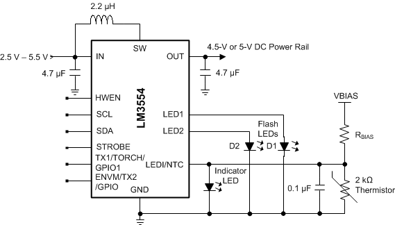
Typical Application Circuit
