SNVS549C June 2009 – February 2016 LM3554
PRODUCTION DATA.
- 1 Features
- 2 Applications
- 3 Description
- 4 Revision History
- 5 Specifications
-
6 Detailed Description
- 6.1 Overview
- 6.2 Functional Block Diagram
- 6.3
Feature Description
- 6.3.1 Start-Up
- 6.3.2 Overvoltage Protection
- 6.3.3 Current Limit
- 6.3.4 Flash Termination (Strobe-Initiated Flash)
- 6.3.5 Flash Termination (I2C-Initiated Flash)
- 6.3.6 Flash Timeout
- 6.3.7 Torch Mode
- 6.3.8 TX1/Torch
- 6.3.9 ENVM/TX2/GPIO2
- 6.3.10 Indicator LED/Thermistor (LEDI/NTC)
- 6.3.11 Alternative External Torch (AET Mode)
- 6.3.12 Input Voltage Monitor
- 6.3.13 LM3554 Timing Diagrams
- 6.3.14 Flags Register and Fault Indicators
- 6.3.15 Thermal Shutdown
- 6.3.16 LED Fault
- 6.3.17 Flash Timeout
- 6.3.18 LED Thermal Fault
- 6.3.19 Input Voltage Monitor Fault
- 6.3.20 TX1 And TX2 Interrupt Flags
- 6.3.21 Light Load Disable
- 6.4 Device Functional Modes
- 6.5 Programming
- 6.6 Register Maps
-
7 Application and Implementation
- 7.1 Application Information
- 7.2
Typical Application
- 7.2.1 Design Requirements
- 7.2.2 Detailed Design Procedure
- 7.2.3 Application Curves
- 8 Power Supply Recommendations
- 9 Layout
- 10Device and Documentation Support
- 11Mechanical, Packaging, and Orderable Information
Package Options
Mechanical Data (Package|Pins)
- YFQ|16
Thermal pad, mechanical data (Package|Pins)
Orderable Information
7 Application and Implementation
NOTE
Information in the following applications sections is not part of the TI component specification, and TI does not warrant its accuracy or completeness. TI’s customers are responsible for determining suitability of components for their purposes. Customers should validate and test their design implementation to confirm system functionality.
7.1 Application Information
The LM3554 is a dual-string white-LED driver for LED camera flash applications. The dual high-side current sources allow for grounded cathode LEDs. The integrated boost provides the power for the current sources and can source up to 1.2 A from a single-cell Li+ voltage range.
7.2 Typical Application
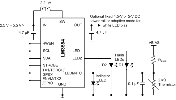 Figure 41. LM3554 Typical Application
7.2.1 Design Requirements
For typical LM3554 device applications, use the parameters listed in Table 10.
Table 10. Design Parameters
| DESIGN PARAMETER | EXAMPLE VALUE |
|---|---|
| Minimum input voltage | 2.5 V |
| Programmable output voltage | 4.5 V or 5 V |
| Programmable output current | 37.5 mA to 1.2 A |
Table 11. Application Circuit Component List
| COMPONENT | MANUFACTURER | VALUE | PART NUMBER | SIZE (mm) | RATING |
|---|---|---|---|---|---|
| L | TOKO | 2.2 µH | FDSE0312-2R2M | 3 × 3 × 1.2 | 2.3 A (0.2 Ω) |
| COUT | Murata | 4.7 µF/10 µF | GRM188R60J475M, or GRM188R60J106M | 0603 (1.6 × 0.8 ×0.8 ) | 6.3 V |
| CIN | Murata | 4.7 µF | GRM185R60J475M | 0603 (1.6 × 0.8 × 0.8 ) | 6.3 V |
| LEDs | Lumiled | LXCL-PWF4 | 1.5 A |
7.2.2 Detailed Design Procedure
7.2.2.1 Output Capacitor Selection
The LM3554 is designed to operate with a at least a 4.7-µF ceramic output capacitor in LED mode and a 10-µF output capacitor in voltage-output mode. When the boost converter is running the output capacitor supplies the load current during the boost converters on-time. When the NMOS switch turns off the inductor energy is discharged through the internal PMOS switch supplying power to the load and restoring charge to the output capacitor. This causes a sag in the output voltage during the on time and a rise in the output voltage during the off time. The output capacitor is therefore chosen to limit the output ripple to an acceptable level depending on load current and input/output voltage differentials and also to ensure the converter remains stable.
For proper LED operation the output capacitor must be at least a 4.7-µF ceramic (10-µF in voltage-output mode). Larger capacitors such as 10 µF or 22 µF can be used if lower output voltage ripple is desired. To estimate the output voltage ripple considering the ripple due to capacitor discharge (ΔVQ) and the ripple due to equivalent series resistance (ESR) of the capacitor (ΔVESR) use Equation 1 and Equation 2:
For continuous conduction mode, the output voltage ripple due to the capacitor discharge is:

The output voltage ripple due to the output capacitors ESR is found by:

In ceramic capacitors the ESR is very low, thus the assumption is that that 80% of the output voltage ripple is due to capacitor discharge and 20% from ESR. Table 12 lists different manufacturers for various output capacitors and their case sizes suitable for use with the LM3554.
7.2.2.2 Input Capacitor Selection
Choosing the correct size and type of input capacitor helps minimize the voltage ripple caused by the device boost converter switching and reduces noise on the devices input terminal that can feed through and disrupt internal analog signals. In the Figure 41 a 4.7-µF ceramic input capacitor works well. It is important to place the input capacitor as close to the device input (IN) terminals as possible. This reduces the series resistance and inductance that can inject noise into the device due to the input switching currents. Table 12 lists various input capacitors that or recommended for use with the LM3554.
Table 12. Recommended Input/Output Capacitors (X5R Dielectric)
| MANUFACTURER | PART NUMBER | VALUE | CASE SIZE (mm) | VOLTAGE RATING |
|---|---|---|---|---|
| TDK Corporation | C1608JB0J475K | 4.7 µF | 0603 (1.6 × 0.8 × 0.8 ) | 6.3 V |
| TDK Corporation | C1608JB0J106M | 10 µF | 0603 (1.6 × 0.8 × 0.8 ) | 6.3 V |
| TDK Corporation | C2012JB1C475K | 4.7 µF | 0805 (2 ×1.25 ×1.25) | 16 V |
| TDK Corporation | C2012JB1A106M | 10 µF | 0805 (2 ×1.25 ×1.25) | 10 V |
| TDK Corporation | C2012JB0J226M | 22 µF | 0805 (2 ×1.25 ×1.25) | 6.3 V |
| Murata | GRM188R60J475KE19 | 4.7 µF | 0603 (1.6 × 0.8 × 0.8 ) | 6.3 V |
| Murata | GRM21BR61C475KA88 | 4.7 µF | 0805 (2 ×1.25 ×1.25) | 16 V |
| Murata | GRM21BR61A106KE19 | 10 µF | 0805 (2 ×1.25 ×1.25) | 10 V |
| Murata | GRM21BR60J226ME39L | 22 µF | 0805 (2 ×1.25 ×1.25) | 6.3 V |
7.2.2.3 Inductor Selection
The LM3554 is designed to use a 2.2-µH inductor. Table 13 lists various inductors and their manufacturers that can work well with the LM3554. When the device is boosting (VOUT > VIN) the inductor is typically the biggest area of efficiency loss in the circuit. Therefore, choosing an inductor with the lowest possible series resistance is important. Additionally, the saturation rating of the inductor must be greater than the maximum operating peak current of the LM3554. This prevents excess efficiency loss that can occur with inductors that operate in saturation and prevents over heating of the inductor and possible damage. For proper inductor operation and circuit performance ensure that the inductor saturation and the peak current limit setting of the LM3554 is greater than IPEAK can be calculated by:

where
- ƒSW = 2 MHz
- η can be found in Typical Characteristics
Table 13. Recommended Inductors
| MANUFACTURER | L | PART NUMBER | DIMENSIONS (L×W×H)(mm) | ISAT |
|---|---|---|---|---|
| TOKO | 2.2 µH | FDSE0312-2R2M | 3 × 3 ×1.2 | 2 A |
| TDK | 2.2 µH | VLS252012T-2R2M1R3 | 2 × 2.5 ×1.2 mm | 1.5 A |
| Coilcraft | 2. 2µH | LPS4018-222ML | 3.9 × 3.9 × 1.7 mm | 2.3 A |
7.2.2.4 NTC Thermistor Selection
NTC thermistors have a temperature to resistance relationship of:

where
- β is given in the thermistor datasheet
- R25C is the thermistors value at 25°C
Figure 43 is chosen so that it is equal to:

where
- R(T)TRIP is the thermistor value at the temperature trip point
- VBIAS is shown in Figure 43
- VTRIP = 1.05V (typical)
Choosing R3 here gives a more linear response around the temperature trip voltage. For example, with VBIAS = 2.5 V, a thermistor whose nominal value at 25°C is 100 kΩ and a β = 4500 K, the trip point is chosen to be 93°C. The value of R(T) at 93°C is:

Figure 42 shows the linearity of the thermistor resistive divider of the previous example.
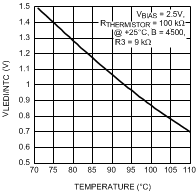 Figure 42. Thermistor Resistive Divider Response vs Temperature
Another useful equation for the thermistor resistive divider is developed by combining the equations for R3, and R(T) and solving for temperature. This is shown in Equation 7:

Using, for example, Excel® spreadsheet software, different curves for the temperature trip point T (°C) can be created vs R3, Beta, or VBIAS in order to help better choose the thermal components for practical values of thermistors, series resistors (R3), or reference voltages VBIAS.
Programming bit [3] of the Configuration Register with a 1 selects thermal comparator mode making the LEDI/NTC pin a comparator input for flash LED thermal sensing. Figure 43 shows the internal block diagram of the thermal sensing circuit which is OR’d with both the TX1 and ENVM/TX2 (TX2 mode) to force the LM3554 from flash to torch mode. This is intended to prevent LED overheating during flash pulses.
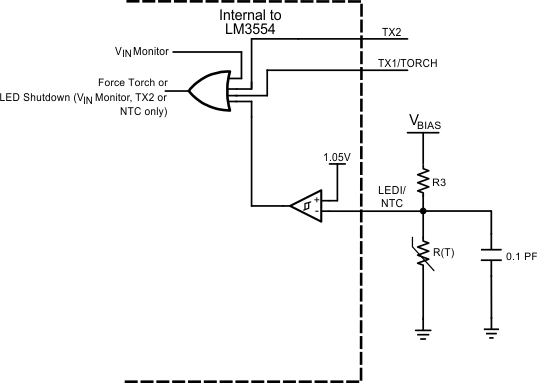 Figure 43. Thermistor Voltage Divider and Sensing Circuit
7.2.2.5 NTC Thermistor Placement
The termination of the thermistor must be done directly to the cathode of the flash LED in order to adequately couple the heat from the LED into the thermistor. Consequently, the noisy environment generated from the boost converter switching can introduce noise from GND into the thermistor sensing input. To filter out this noise it is necessary to place a 0.1-µF or larger ceramic capacitor close to the LEDI/NTC pin. The filter capacitor's return must also connect with a low-impedance trace, as close to the PGND pin of the device as possible.
7.2.2.6 Maximum Load Current (Voltage Mode)
Assuming the power dissipation in the LM3554 and the ambient temperature are such that the device does not hit thermal shutdown, the maximum load current as a function of IPEAK is:

where
- η is efficiency and is found in the efficiency curves in the Typical Characteristics
and

Figure 44 shows the theoretical maximum output current vs theoretical efficiency at different input and output voltages using Equation 8 and Equation 9 for ΔIL and ILOAD with a peak current of 2.5 A. Figure 44 represents the theoretical maximum output current (for the LM3554 in voltage-output mode) that the device can deliver just before hitting current limit.
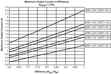 Figure 44. LM3554 Maximum Output Current
7.2.2.7 Maximum Output Power
Output power is limited by three things: the peak current limit, the ambient temperature, and the maximum power dissipation in the package. If the LM3554’s die temperature is below the absolute maximum rating of 125°C, the maximum output power can be over 6 W. However, any appreciable output current causes the internal power dissipation to increase and therefore increase the die temperature. This can be additionally compounded if the LED current sources are operating while the device is in voltage-output mode because the difference between VOUT and VLED is dropped across the current sources. Any circuit configuration must ensure that the die temperature remains below 125°C taking into account the ambient temperature derating.
7.2.2.7.1 Voltage-Output Mode
In voltage-output mode the total power dissipated in the LM3554 can be approximated as:

where
- PN is the power lost in the NFET
- PP is the PFET power loss
- PLED1, PLED2, and PIND are the losses across the current sink
An approximate calculation of these losses gives:

Equation 11 consider the average current through the NFET and PFET. The actual power losses are higher due to the RMS currents and the quiescent power into IN. These, however, can give a decent approximation.
7.2.2.7.2 LED Boost Mode
In LED mode with VOUT > VIN the device boost converter switches and make VOUT = VLED + 0.3 V. In this situation the total power dissipated in the LM3554 is approximated as:

7.2.2.7.3 LED Pass Mode
In LED mode with VIN – ILOAD × RPFET > VLED + 0.3 V, the LM3554 operates in pass mode. In this case, the NFET is off, and the PFET is fully on. The difference between VIN - ILOAD × RPMOS and VLED are dropped across the current sources. In this situation the total power dissipated in the LM3554 is approximated as:

Once the total power dissipated in the LM3554 is calculated the ambient temperature and the thermal resistance of the 16-pin DSBGA (YFQ package) are used to calculate the total die temperature (or junction temperature TJ).
As an example, assume the LM3554 is operating at VIN = 3.6 V and configured for voltage-output mode with VOUT = 5 V and IOUT = 0.7 A. The LED currents are then programmed in torch mode with 150 mA each at VLED = 3.6 V. Additionally, the indicator LED has 10 mA at VIND = 3.6 V. Using Equation 12 and Equation 13 above, the approximate total power dissipated in the device is:

The die temperature approximation is:

In this case the device can operate at these conditions. If then the ambient temperature is increased to 85°C, the die temperature would be 140.8°C; thus, the die temperature would be above the absolute maximum ratings, and the load current would need to be scaled back. This example demonstrates the steps required to estimate the amount of current derating based upon operating mode, circuit parameters, and the device's junction-to-ambient thermal resistance. In this example a thermal resistance of 75.8°C/W was used (JESD51-7 standard). Because thermal resistance from junction-to-ambient is largely PCB layout dependent, the actual number used likely may be different and must be taken into account when performing these calculations.
7.2.3 Application Curves
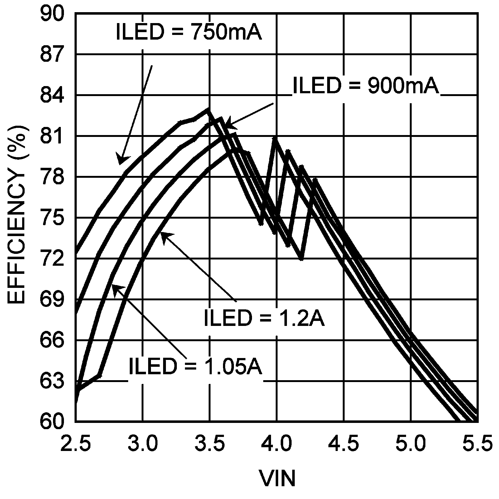
| Single LED |
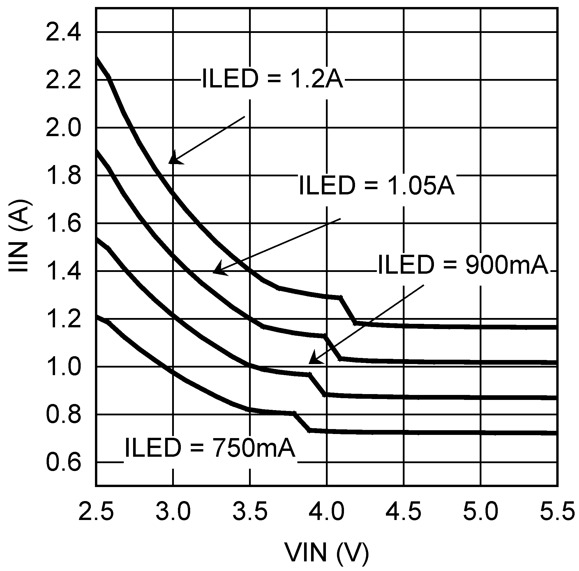
| Single LED |
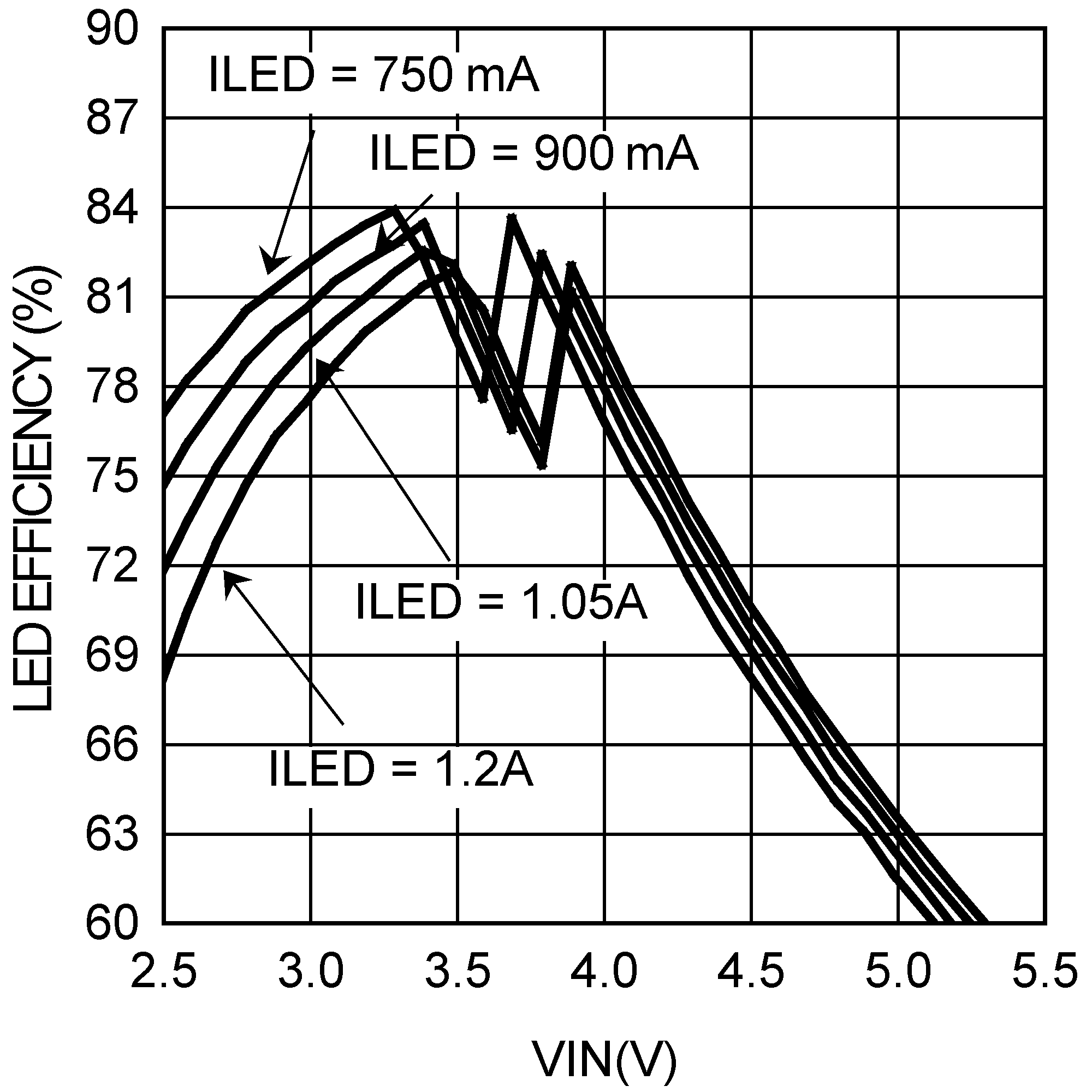
| Dual LEDs | L = Coilcraft LPS4018-222 | |
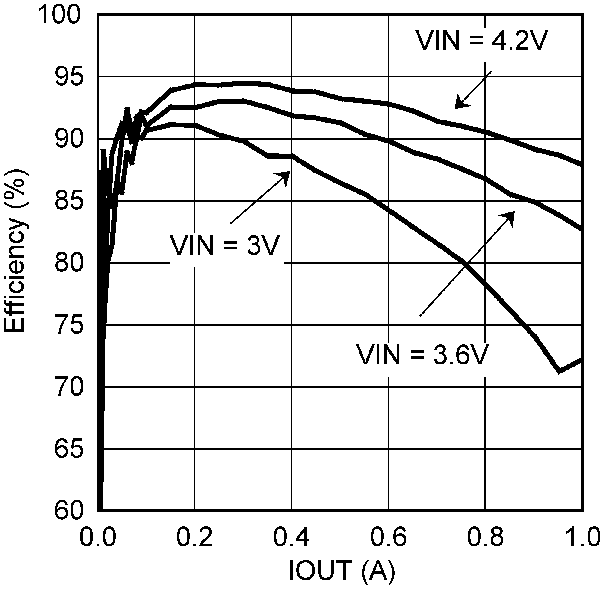
| VOUT = 5 V | Voltage-Output Mode | |
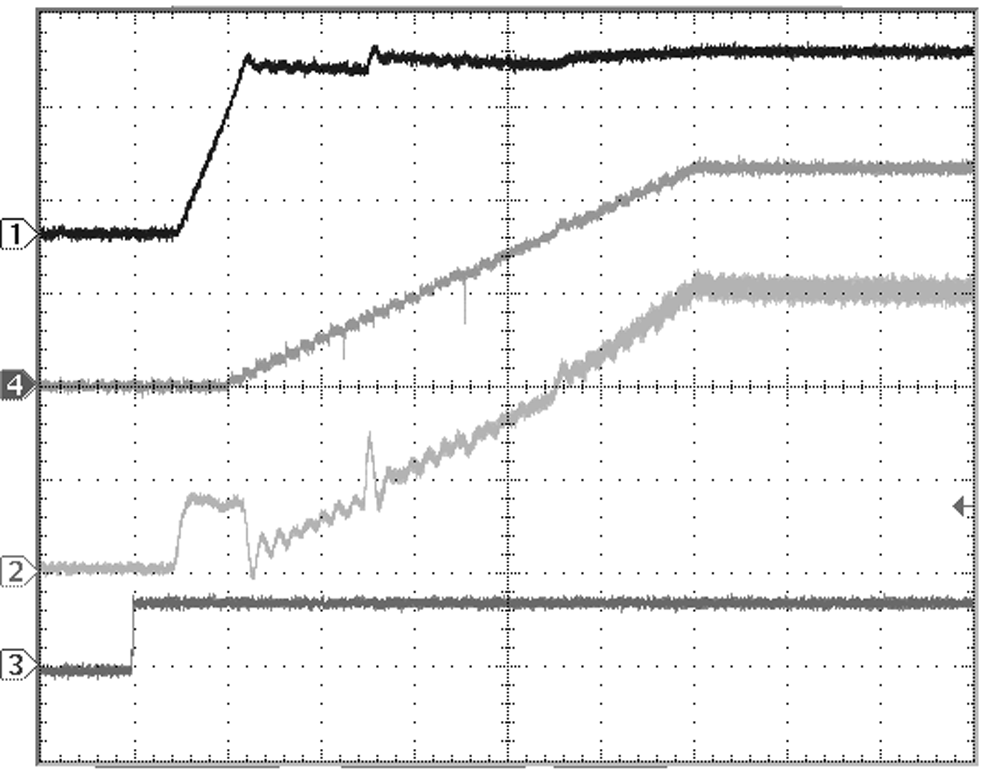
| Time Base: 100 µs/div | IFLASH = 1.2 A | Single LED |
| Ch 1: VOUT (2 V/div) | Ch 2: IL (500 mA/div) | |
| Ch 4: ILED (500 mA/div) | Ch 3: STROBE (5 V/div) | |
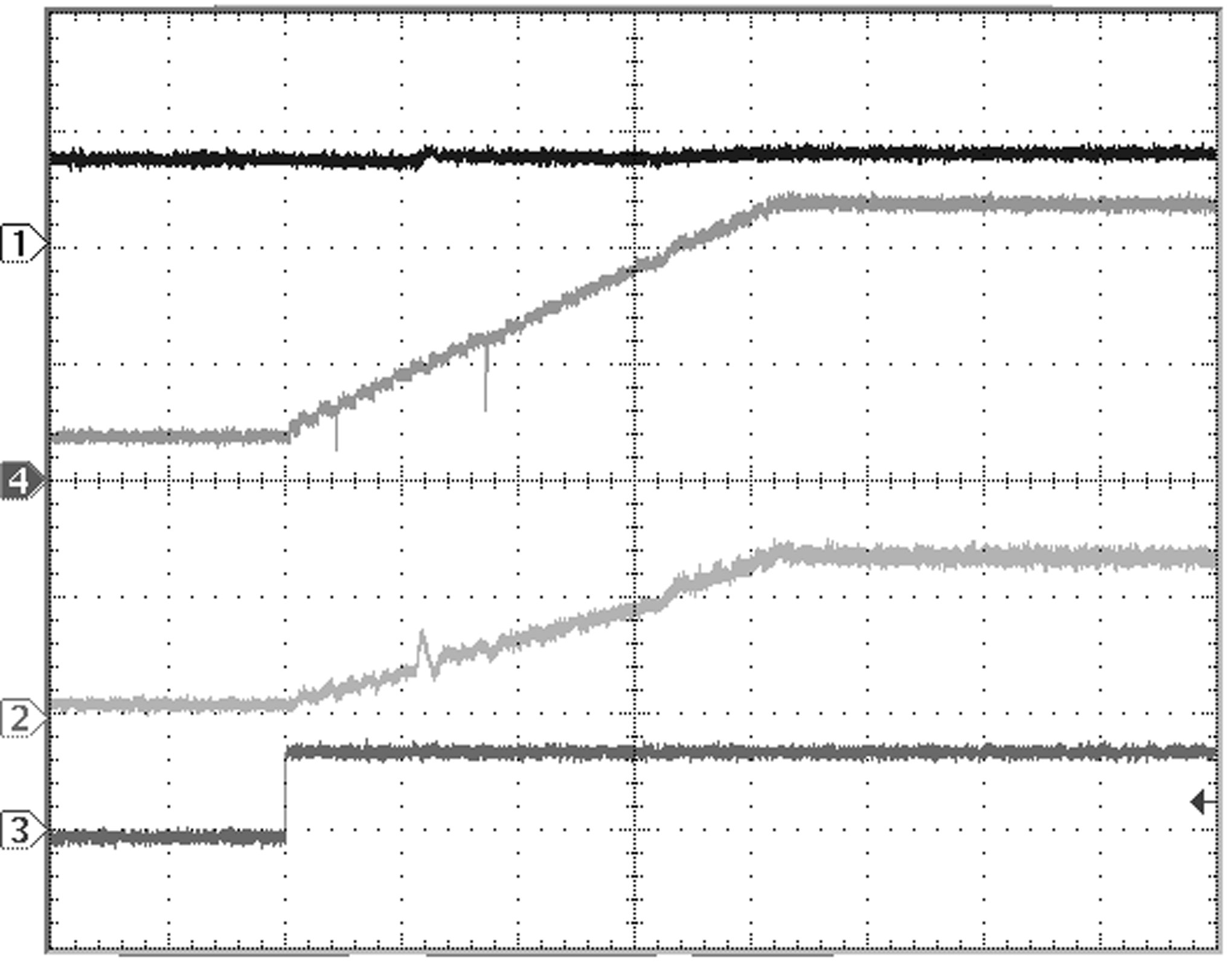
| Time Base: 100 µs/div | IFLASH = 1.2 A | ITORCH = 295 mA |
| Ch 1: VOUT (5 V/div) | Ch 2: IL (1 A/div) | Single LED |
| Ch 4: ILED (500 mA/div) | Ch 3: STROBE (5 V/div) | |
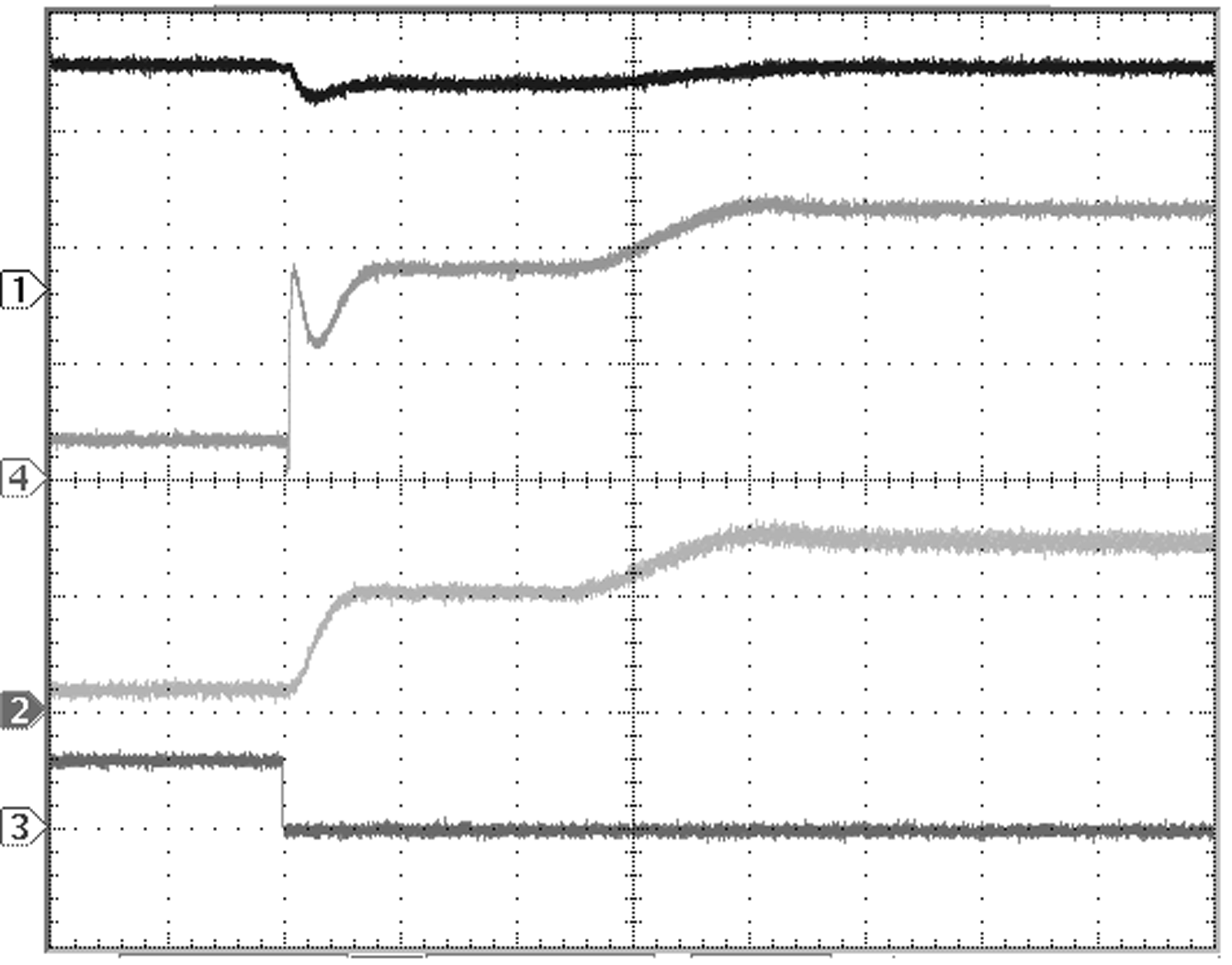
| Time Base: 20 µs/div | IFLASH = 1.2 A | ITORCH = 180 mA |
| Ch 1: VOUT (2 V/div) | Ch 2: IL (1 A/div) | Single LED |
| Ch 4: ILED (500 mA/div) | ||
| Ch 3: TX1 (5 V/div) | ||
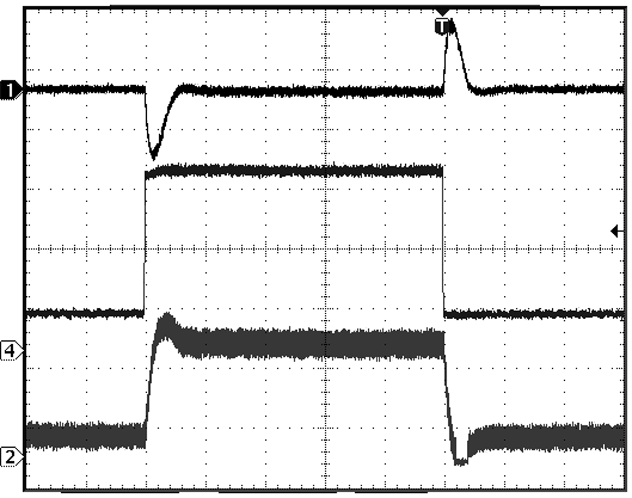
| Time Base: 40 µs/div | VIN = 3.6 V | VOUT = 5 V |
| Ch 1: VOUT (500 mV/div) | Ch 2: IL (500 mA/div) | |
| Ch 4: IOUT (500 mA/div) | ||
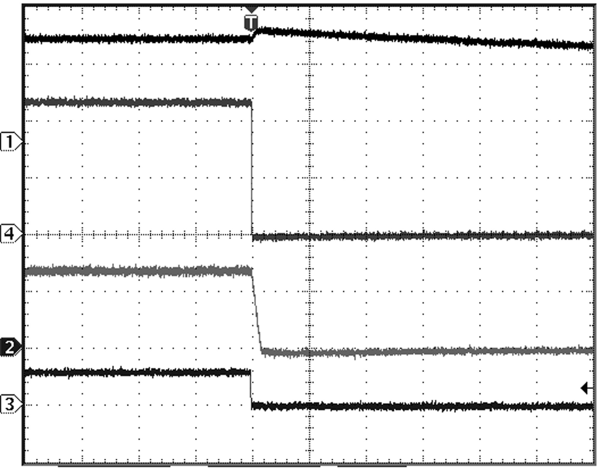
| Time Base: 20 µs/div | ILED = 1.2 A | Single LED |
| Ch 1: VOUT (2 V/div) | Ch 3: HWEN (5 V/div) | |
| Ch 4: ILED (500 mA/div) | ||
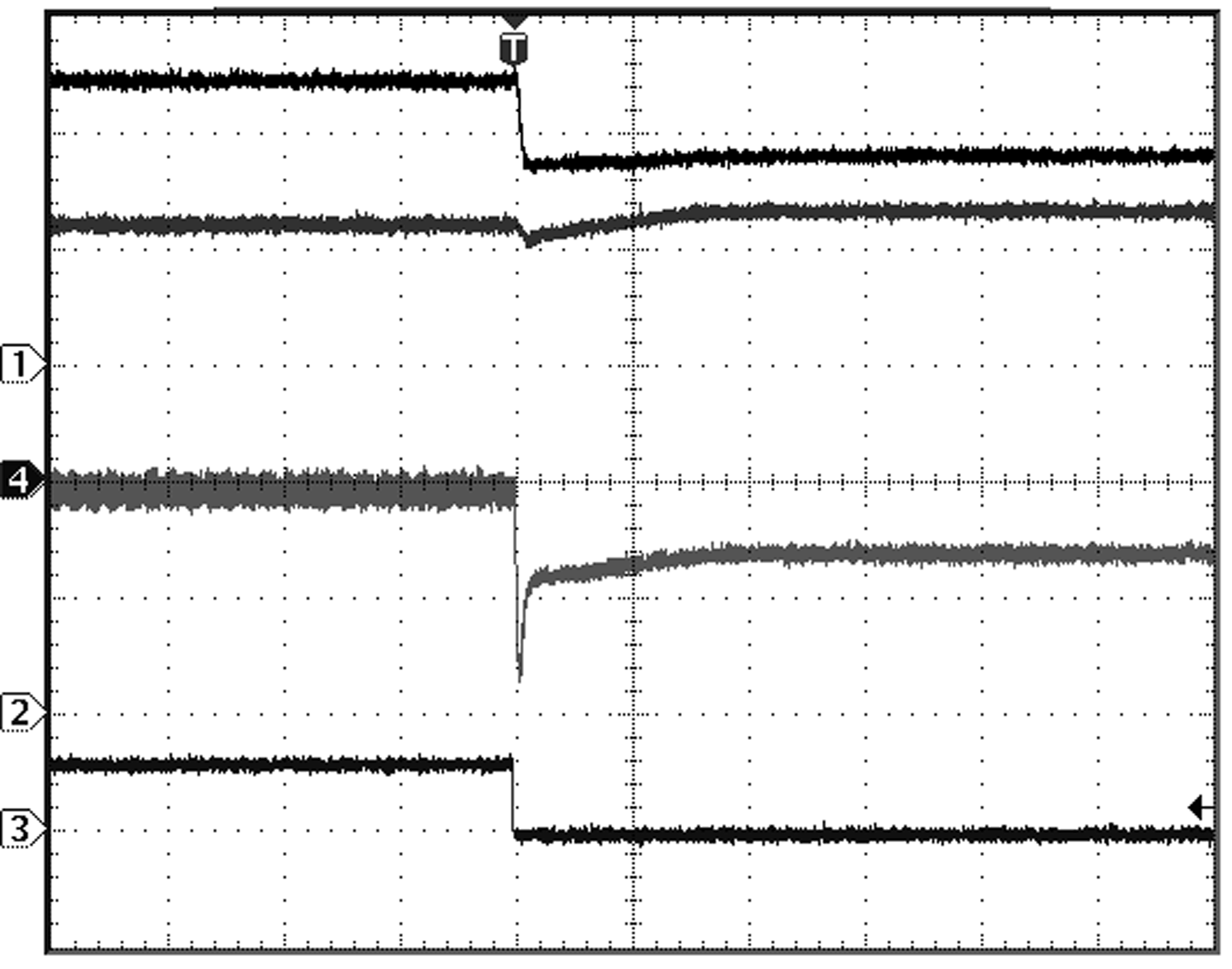
| Time Base: 100 µs/div | ILED = 1.2 A | VOUT = 5 V |
| Ch 1: VOUT (2 V/div) | Ch 2: IL (1 A/div) | Single LED |
| Ch 4: ILED (500mA/div) | Ch 3: ENVM (5 V/div) | |
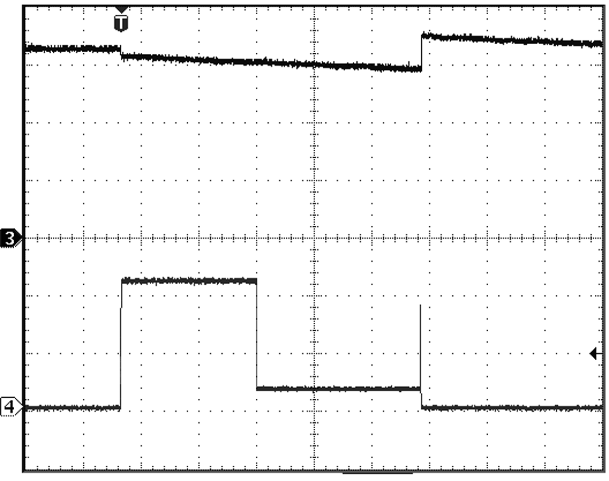
| Time Base: 100 ms/div | ILED = 1.2 A | 3.1-V UVLO Setting | ||
| Ch 3: VIN (1V/div) | Ch 4: ILED (500 mA/div) | Single LED |
| Dual LEDs |
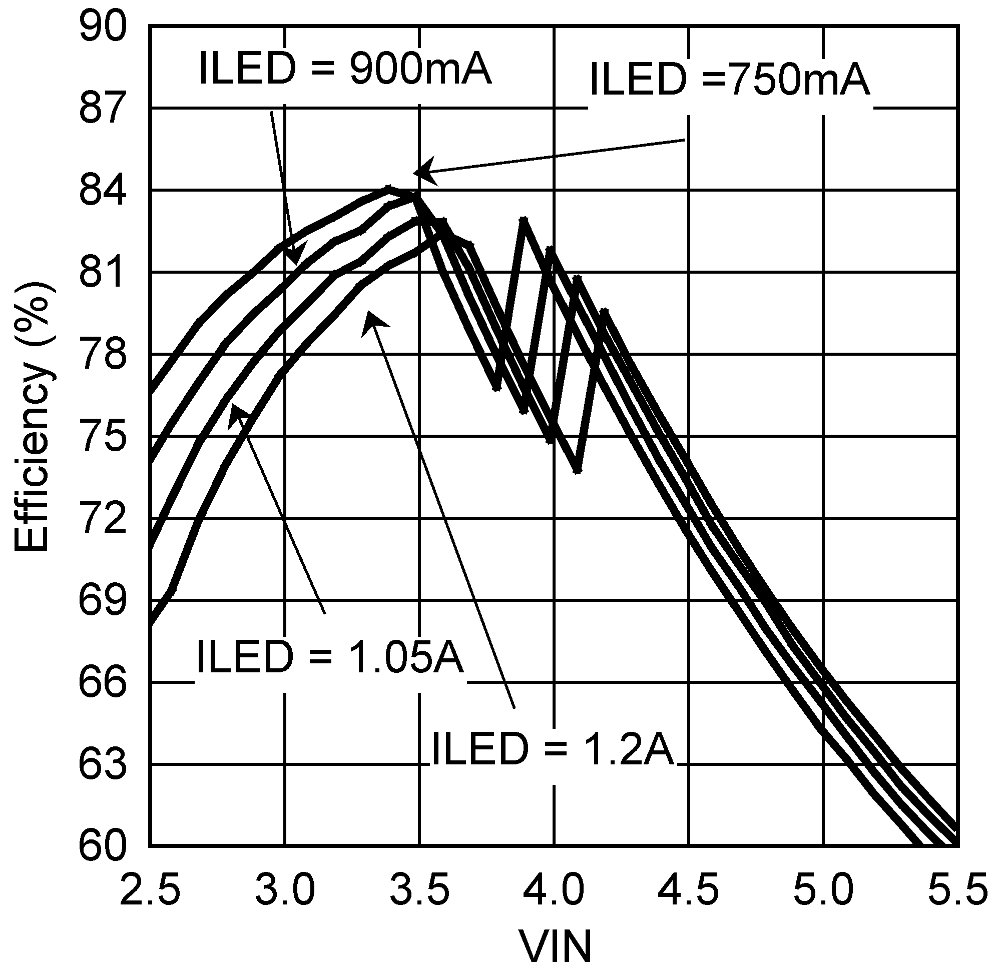
| Single LED | L = Coilcraft LPS4018-222 | |
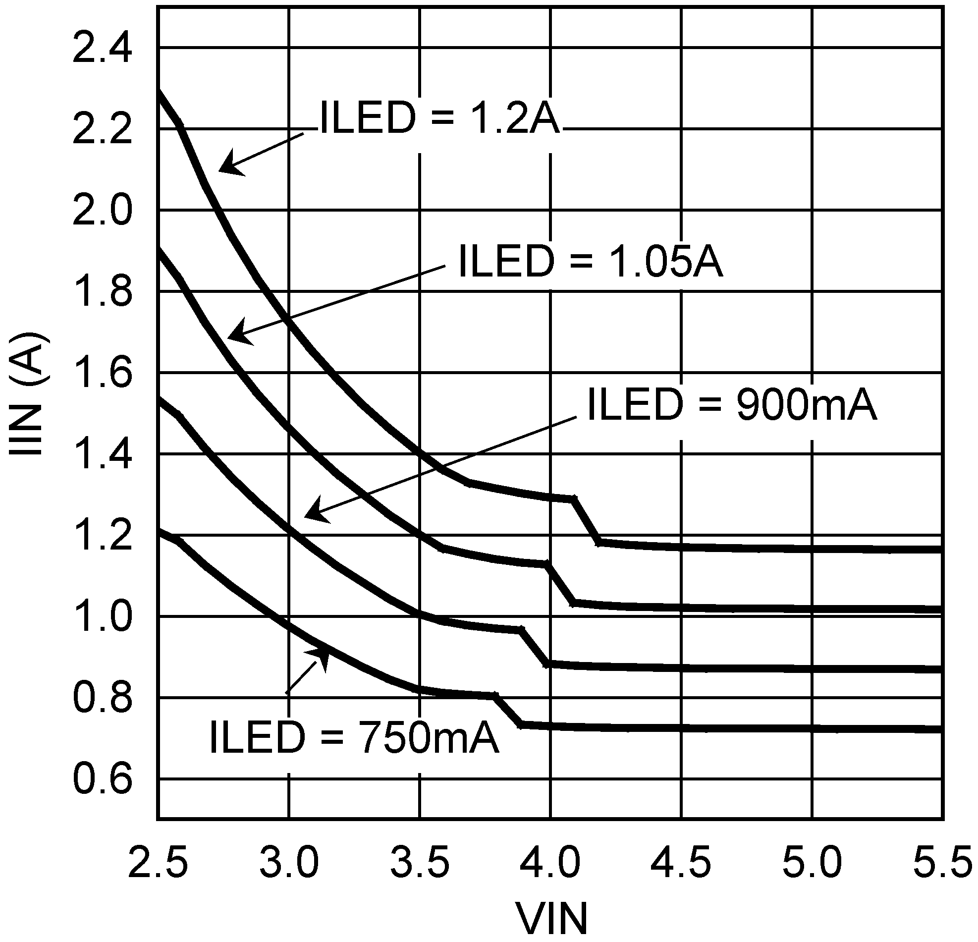
| Single LED | L = Coilcraft LPS4018-222 | |
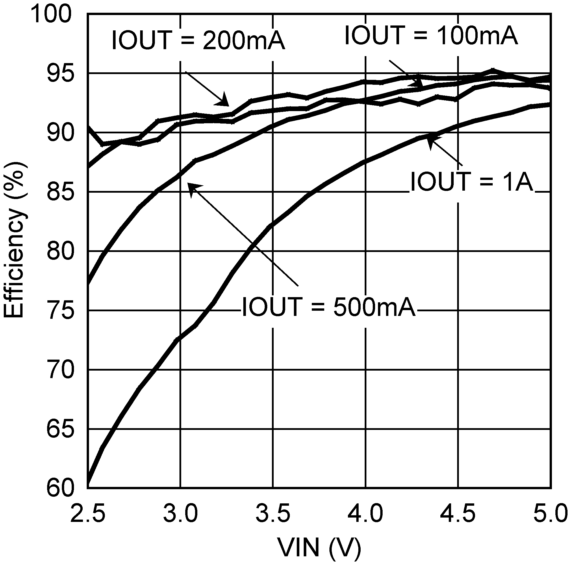
| VOUT = 5 V | Voltage-Output Mode | |
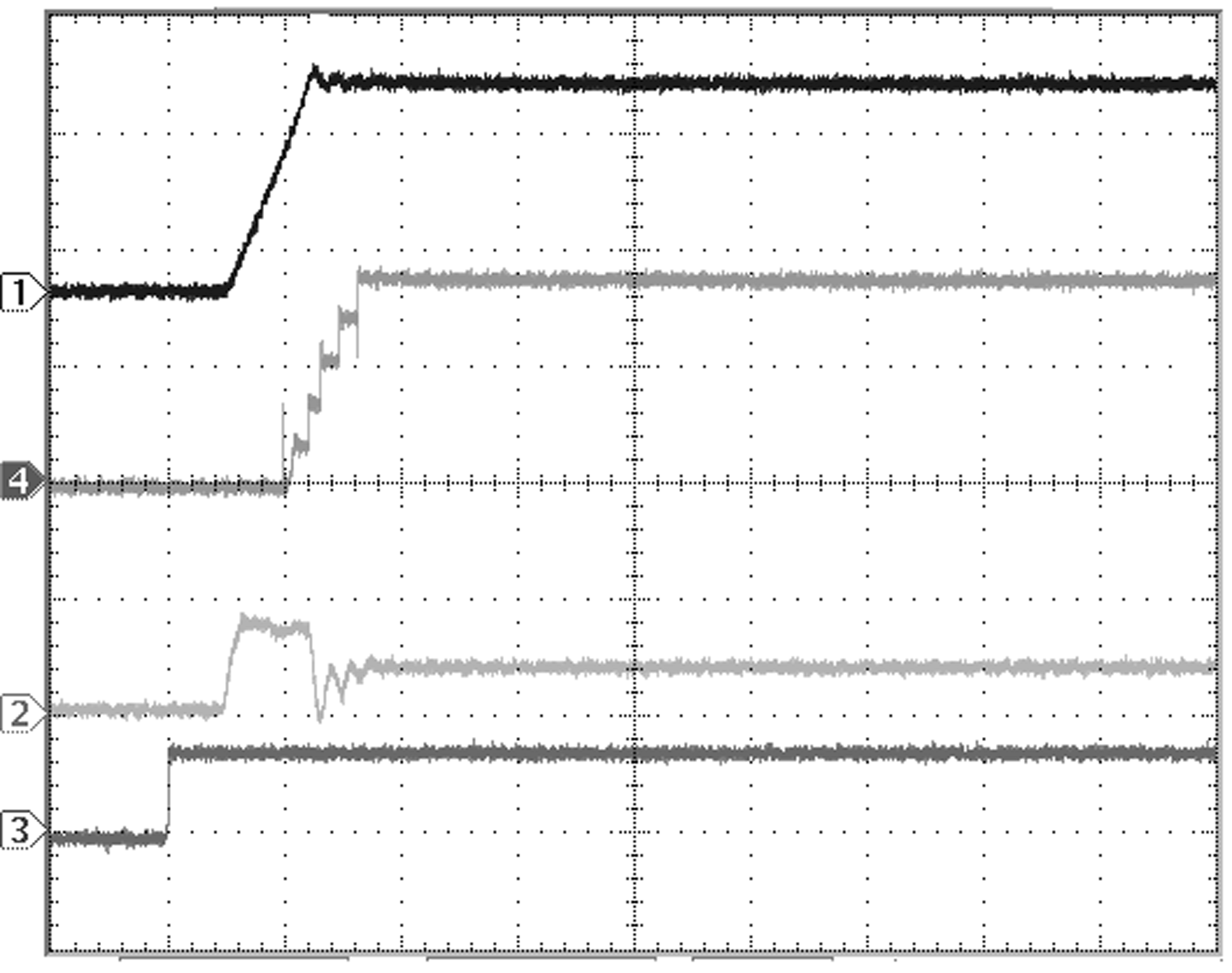
| Time Base: 100 µs/div | ITORCH = 180 mA | |
| 90-mA Torch Setting | Single LED | |
| Chl 1: VOUT (2 V/div) | Ch 2: IL (500 mA/div) | |
| Ch 4: ILED (100 mA/div) | Ch 3: TX1 (5 V/div) | |
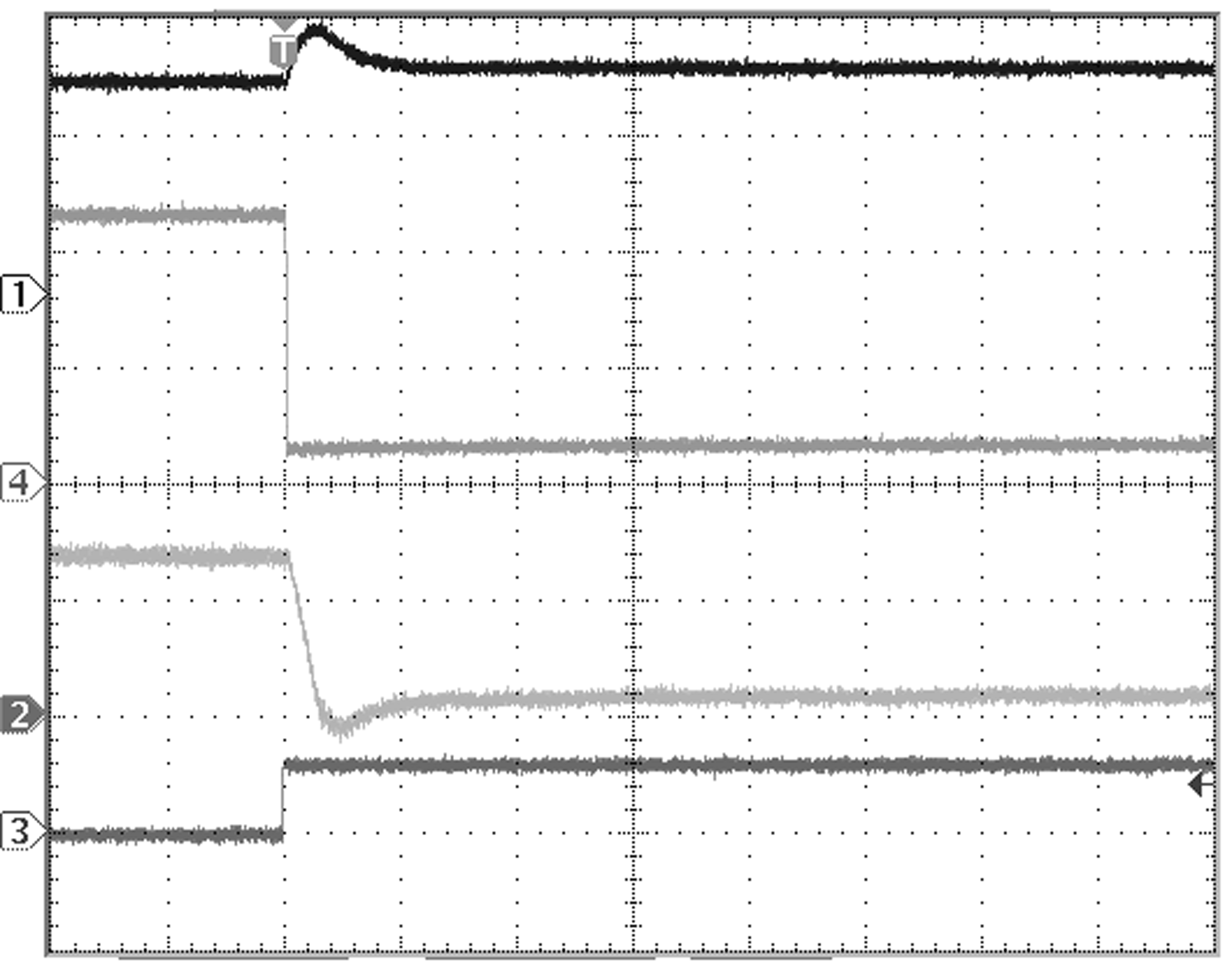
| Time Base: 20 µs/div | IFLASH = 1.2 A | ITORCH = 180 mA |
| Ch 1: VOUT (2 V/div) | Ch 2: IL (1 A/div) | Single LED |
| Ch 4: ILED (500 mA/div) | Ch 3: TX1 (5 V/div) | |
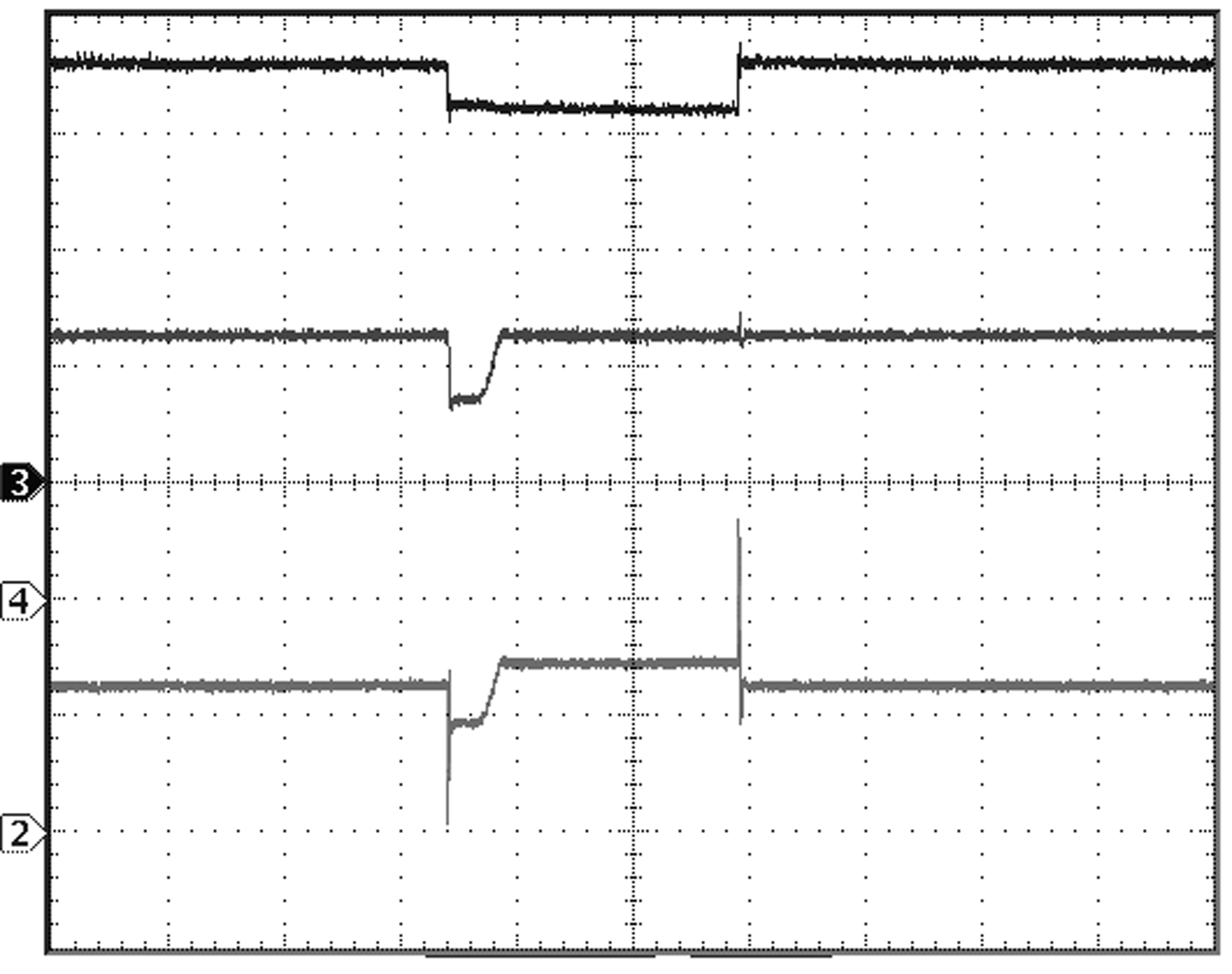
| Time Base: 400 µs/div | IFLASH = 1.2 A | Single LED |
| Ch 3: VIN (5 V/div) | Ch 2: IL (1 A/div) | |
| Ch 4: ILED (500 mA/div) | ||
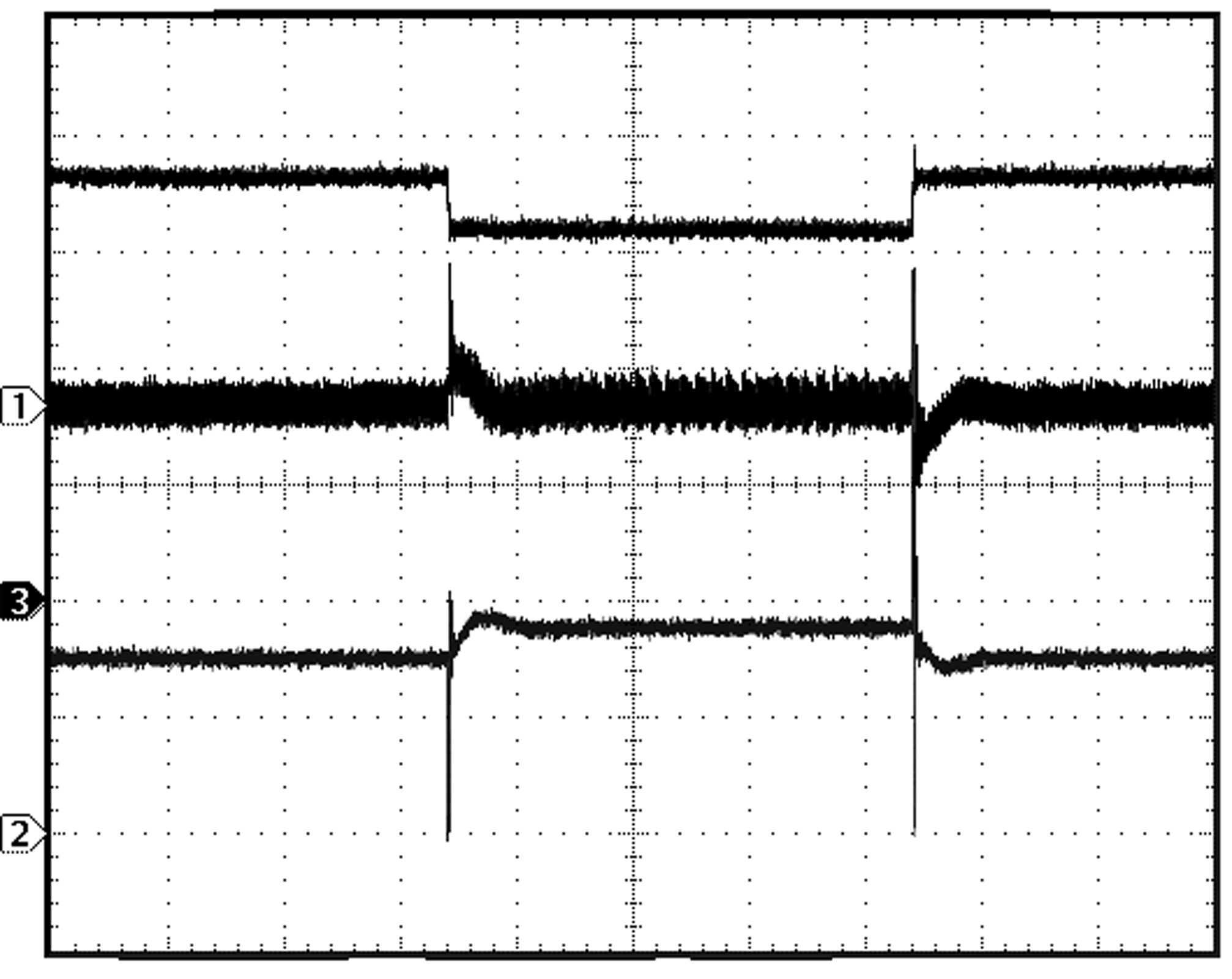
| Time Base: 200 µs/div | VOUT = 5 V | IOUT = 500 mA |
| Ch 1: VOUT = (5 V/div) | Ch 2: IL + IIN (500 mA/div) | |
| Ch 3 (Top Trace): VIN (1 V/div) | ||
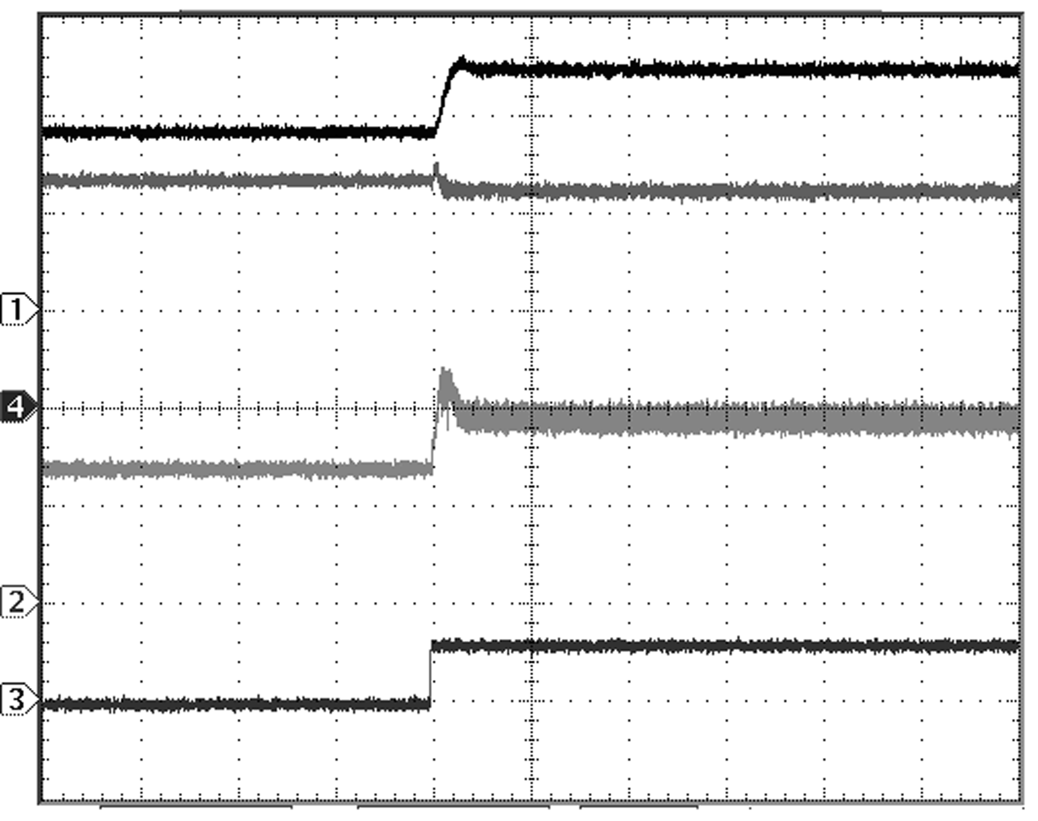
| Time Base: 100 µs/div | VOUT = 5 V | ILED = 1.2 A |
| Ch 1: VOUT (2 V/div) | Ch 2: IL (1 A/div) | Single LED |
| Ch 4: ILED (500 mA/div) | Ch 3: ENVM (5 V/div) | |
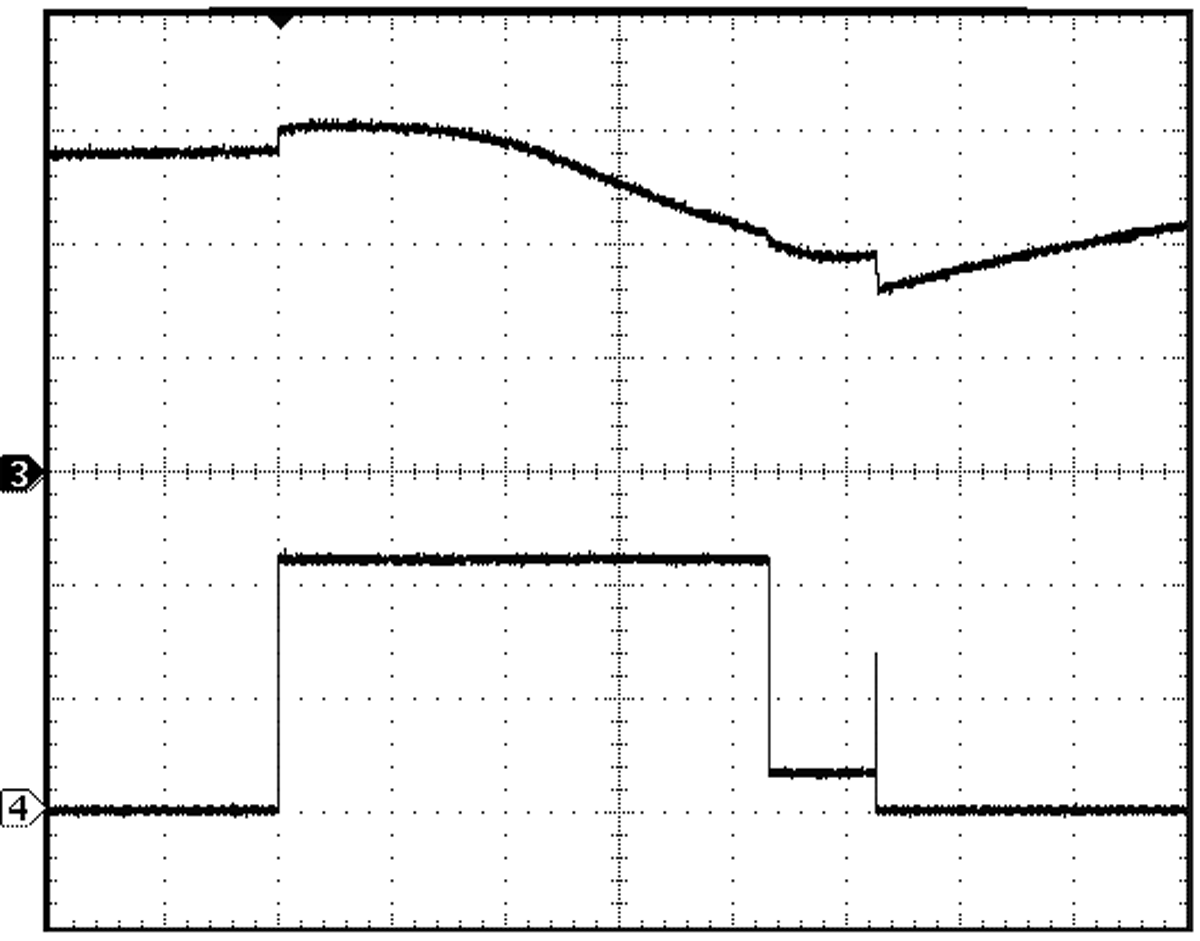
| Time Base: 200 µs/div | Circuit of Figure 43 | |
| Single LED | ILED = 1.2 A | |
| Ch 3: NTC pin voltage (5 V/div) | Ch 4: ILED (500 mA/div) | |
| R(T) = 100 kΩ at 25°C | R3 = 9 kΩ | |