SNVS821A January 2014 – March 2014 LM3699
PRODUCTION DATA.
- 1 Features
- 2 Applications
- 3 Description
- 4 Revision History
- 5 Terminal Configuration and Functions
- 6 Specifications
- 7 Detailed Description
- 8 Application and Implementation
- 9 Power Supply Recommendations
- 10Layout
- 11Device and Documentation Support
- 12Mechanical, Packaging, and Orderable Information
Package Options
Mechanical Data (Package|Pins)
- YFQ|12
Thermal pad, mechanical data (Package|Pins)
Orderable Information
1 Features
- Drives Parallel High-Voltage LED Strings for Display or Keypad Lighting
- Boost Converter up to 90% Efficiency
- Four User-Selectable Full-Scale Current Settings
(20.2 mA, 18.6 mA, 17.0 mA, 15.4 mA) - Quick-Dimming Enable Terminal (ILOW)
- Simple PWM Duty Cycle Control
- 24-V Overvoltage Protection Threshold
- Fixed 1-MHz Switching Frequency
- Integrated 1-A/40-V MOSFET
- Three Current Sink Terminals
- Adaptive Boost Output to LED Voltages
- Thermal Shutdown Protection
- 29-mm2 Total Solution Size
2 Applications
- Power Source for Smart Phone Illumination
- Display or Keypad Illumination
3 Description
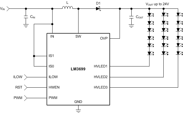
The LM3699 is a three-string, high-efficiency, PWM-controlled power source for display backlight or keypad LEDs in smartphone handsets. The high-voltage inductive boost converter with integrated 1-A, 40-V MOSFET provides the power for three series LED strings. The boost output automatically adjusts to LED forward voltage to minimize headroom voltage and effectively improve LED efficiency.
The ILOW terminal provides a method to quickly reduce LED brightness during camera flash operation.
The LM3699 has integrated overvoltage, overcurrent, and thermal protection.
The device operates over a 2.7-V to 5.5-V input voltage range and a −40°C to 85°C temperature range.
Device Information
| ORDER NUMBER | PACKAGE | BODY SIZE |
|---|---|---|
| LM3699YFQ | DSBGA (12) | 1,64 mm x 1,29 mm |
Simplified Schematic