SNVSA44B August 2014 – January 2018 LM43601
PRODUCTION DATA.
- 1 Features
- 2 Applications
- 3 Description
- 4 Revision History
- 5 Pin Configuration and Functions
- 6 Specifications
-
7 Detailed Description
- 7.1 Overview
- 7.2 Functional Block Diagram
- 7.3
Feature Description
- 7.3.1 Fixed-Frequency, Peak-Current-Mode Controlled, Step-Down Regulator
- 7.3.2 Light Load Operation
- 7.3.3 Adjustable Output Voltage
- 7.3.4 Enable (ENABLE)
- 7.3.5 VCC, UVLO and BIAS
- 7.3.6 Soft Start and Voltage Tracking (SS/TRK)
- 7.3.7 Switching Frequency (RT) and Synchronization (SYNC)
- 7.3.8 Minimum ON-Time, Minimum OFF-Time, and Frequency Foldback at Dropout Conditions
- 7.3.9 Internal Compensation and CFF
- 7.3.10 Bootstrap Voltage (BOOT)
- 7.3.11 Power Good (PGOOD)
- 7.3.12 Overcurrent and Short-Circuit Protection
- 7.3.13 Thermal Shutdown
- 7.4 Device Functional Modes
-
8 Applications and Implementation
- 8.1 Application Information
- 8.2
Typical Application
- 8.2.1 Design Requirements
- 8.2.2
Detailed Design Procedure
- 8.2.2.1 Custom Design With WEBENCH® Tools
- 8.2.2.2 Output Voltage Setpoint
- 8.2.2.3 Switching Frequency
- 8.2.2.4 Input Capacitors
- 8.2.2.5 Inductor Selection
- 8.2.2.6 Output Capacitor Selection
- 8.2.2.7 Feedforward Capacitor
- 8.2.2.8 Bootstrap Capacitors
- 8.2.2.9 VCC Capacitor
- 8.2.2.10 BIAS Capacitors
- 8.2.2.11 Soft-Start Capacitors
- 8.2.2.12 Undervoltage Lockout Set-Point
- 8.2.2.13 PGOOD
- 8.2.3 Application Curves
- 9 Power Supply Recommendations
- 10Layout
- 11Device and Documentation Support
- 12Mechanical, Packaging, and Orderable Information
Package Options
Mechanical Data (Package|Pins)
- PWP|16
Thermal pad, mechanical data (Package|Pins)
- PWP|16
Orderable Information
7.3.1 Fixed-Frequency, Peak-Current-Mode Controlled, Step-Down Regulator
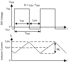
This description of the LM43601 refer to the Functional Block Diagram and to the waveforms in Figure 33. The LM43601 is a step-down buck regulator with both high-side (HS) switch and low-side (LS) switch (synchronous rectifier) integrated. The LM43601 supplies a regulated output voltage by turning on the HS and LS NMOS switches with controlled ON-time. During the HS switch ON-time, the SW pin voltage VSW swings up to approximately VIN, and the inductor current IL increases with a linear slope (VIN – VOUT) / L. When the HS switch is turned off by the control logic, the LS switch is turned on after a anti-shoot-through dead time. Inductor current discharges through the LS switch with a slope of –VOUT / L. The control parameter of buck converters are defined as duty cycle D = tON / TSW, where tON is the HS switch ON time and TSW is the switching period. The regulator control loop maintains a constant output voltage by adjusting the duty cycle D. In an ideal buck converter, where losses are ignored, D is proportional to the output voltage and inversely proportional to the input voltage: D = VOUT / VIN.
 Figure 33. SW Node and Inductor Current Waveforms in Continuous Conduction Mode (CCM)
The LM43601 synchronous buck converter employs peak current mode control topology. A voltage feedback loop is used to get accurate DC voltage regulation by adjusting the peak-current command based on voltage offset. The peak-inductor current is sensed from the HS switch and compared to the peak current to control the ON-time of the HS switch. The voltage feedback loop is internally compensated, which allows for fewer external components, makes it easy to design, and provides stable operation with almost any combination of output capacitors. The regulator operates with fixed switching frequency in CCM and discontinuous conduction mode (DCM). At very light load, the LM43601 operates in PFM to maintain high efficiency, and the switching frequency decreases with reduced load current.