SNVS533D September 2007 – November 2014 LM4510
PRODUCTION DATA.
- 1 Features
- 2 Applications
- 3 Description
- 4 Revision History
- 5 Pin Configuration and Functions
- 6 Specifications
- 7 Detailed Description
-
8 Application and Implementation
- 8.1 Application Information
- 8.2
Typical Applications
- 8.2.1
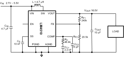
2.7 V to 5.5 V Input with a 16 V Output
- 8.2.1.1 Design Requirements
- 8.2.1.2
Detailed Design Procedure
- 8.2.1.2.1 Adjusting Output Voltage
- 8.2.1.2.2 Maximum Output Current
- 8.2.1.2.3 Inductor Selection
- 8.2.1.2.4 IL_AVE Check
- 8.2.1.2.5 Input Capacitor Selection
- 8.2.1.2.6 Output Capacitor Selection
- 8.2.1.2.7 Soft-Start Function and Soft-Start Capacitor Selection
- 8.2.1.2.8 Compensation Component Selection
- 8.2.1.3 Application Curves
- 8.2.2 Flash and Torch Application
- 8.2.1
2.7 V to 5.5 V Input with a 16 V Output
- 9 Power Supply Recommendations
- 10Layout
- 11Device and Documentation Support
- 12Mechanical, Packaging, and Orderable Information
Package Options
Mechanical Data (Package|Pins)
- DSC|10
Thermal pad, mechanical data (Package|Pins)
- DSC|10
Orderable Information
1 Features
- 18 V@ 80 mA from 3.2 V Input
- 5 V @ 280 mA from 3.2 V Input
- No External Schottky Diode Required
- 85% Peak Efficiency
- Soft Start
- True Shutdown Isolation
- Stable with Small Ceramic or Tantalum Output Capacitors
- Output Short-Circuit Protection
- Feedback Fault Protection
- Input Undervoltage Lock Out
- Thermal Shutdown
- 0.002-µA Shutdown Current
- Wide Input Voltage Range: 2.7 V to 5.5 V
- 1-MHz Fixed Frequency Operation
- Low-profile 10-pin WSON Package (3 mm x 3 mm x 0.8 mm)
2 Applications
- Organic LED Panel Power Supply
- Charging Holster
- White LED Backlight
- USB Power Supply
- Class D Audio Amplifier
- Camera Flash LED Driver
3 Description
The LM4510 is a current mode step-up DC/DC converter with a 1.2-A internal NMOS switch designed to deliver up to 120 mA at 16 V from a Li-Ion battery.
The device's synchronous switching operation (no external Schottky diode) at heavy-load, and non-synchronous switching operation at light-load, maximizes power efficiency.
True shutdown function by synchronous FET and related circuitry ensures input and output isolation.
A programmable soft-start circuit allows the user to limit the amount of inrush current during start-up. The output voltage can be adjusted by external resistors.
The LM4510 features advanced short-circuit protection to maximize safety during output to ground short condition. During shutdown the feedback resistors and the load are disconnected from the input to prevent leakage current paths to ground.
Device Information(1)
| PART NUMBER | PACKAGE | BODY SIZE (NOM) |
|---|---|---|
| LM4510 | WSON (10) | 3.00 mm x 3.00 mm |
- For all available packages, see the orderable addendum at the end of the datasheet.
Typical Application Circuit
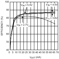
Efficiency at VOUT = 16 V