SNAS470E October 2008 – November 2015 LM48100Q-Q1
PRODUCTION DATA.
- 1 Features
- 2 Applications
- 3 Description
- 4 Revision History
- 5 Pin Configuration and Functions
-
6 Specifications
- 6.1 Absolute Maximum Ratings
- 6.2 ESD Ratings
- 6.3 Recommended Operating Conditions
- 6.4 Thermal Information
- 6.5 Electrical Characteristics for VDD = 5 V
- 6.6 Electrical Characteristics for VDD = 5 V at Extended Temperature Limits
- 6.7 Electrical Characteristics for VDD = 3.6 V
- 6.8 Electrical Characteristics for VDD = 3.6 V at Extended Temperature Limits
- 6.9 I2C Interface Characteristics for VDD = 5 V, 2.2 V ≤ I2C VDD ≤ 5.5 V
- 6.10 I2C Interface Characteristics for VDD = 5 V, 1.8 V ≤ I2C VDD ≤ 2.2 V
- 6.11 Typical Characteristics
-
7 Detailed Description
- 7.1 Overview
- 7.2 Functional Block Diagram
- 7.3 Feature Description
- 7.4 Device Functional Modes
- 7.5 Programming
- 7.6 Register Maps
- 8 Application and Implementation
- 9 Power Supply Recommendations
- 10Layout
- 11Device and Documentation Support
- 12Mechanical, Packaging, and Orderable Information
Package Options
Mechanical Data (Package|Pins)
- PWP|14
Thermal pad, mechanical data (Package|Pins)
- PWP|14
Orderable Information
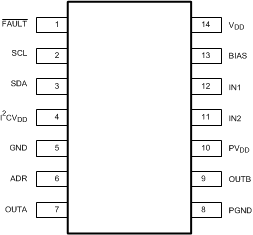
5 Pin Configuration and Functions
PWP Package
14-Pin HTSSOP with PowerPAD
Top View

Pin Functions
| PIN | I/O | DESCRIPTION | |
|---|---|---|---|
| NO. | NAME | ||
| 1 | FAULT | O | Open-Drain output fault flag. FAULT = 0 indicates that a fault condition has occurred. |
| 2 | SCL | I | I2C Clock Input |
| 3 | SDA | I/O | I2C Serial Data Input |
| 4 | I2CVDD | — | I2C Interface Power Supply |
| 5 | GND | — | Ground |
| 6 | ADR | I | I2C Address Bit. Connect to I2CVDD to set address bit, B1 = 1. Connect to GND to set address bit B1 = 0 |
| 7 | OUTA | O | Non-Inverting Audio Output |
| 8 | PGND | — | Power Ground |
| 9 | OUTB | O | Inverting Audio Output |
| 10 | PVDD | — | Output Amplifier Power Supply |
| 11 | IN2 | I | Audio Input 2 |
| 12 | IN1 | I | Audio Input 1 |
| 13 | BIAS | — | Bias Bypass |
| 14 | VDD | — | Power Supply |
| — | Exposed Pad | — | Exposed paddle. Connect to GND. |