SNAS470E October 2008 – November 2015 LM48100Q-Q1
PRODUCTION DATA.
- 1 Features
- 2 Applications
- 3 Description
- 4 Revision History
- 5 Pin Configuration and Functions
-
6 Specifications
- 6.1 Absolute Maximum Ratings
- 6.2 ESD Ratings
- 6.3 Recommended Operating Conditions
- 6.4 Thermal Information
- 6.5 Electrical Characteristics for VDD = 5 V
- 6.6 Electrical Characteristics for VDD = 5 V at Extended Temperature Limits
- 6.7 Electrical Characteristics for VDD = 3.6 V
- 6.8 Electrical Characteristics for VDD = 3.6 V at Extended Temperature Limits
- 6.9 I2C Interface Characteristics for VDD = 5 V, 2.2 V ≤ I2C VDD ≤ 5.5 V
- 6.10 I2C Interface Characteristics for VDD = 5 V, 1.8 V ≤ I2C VDD ≤ 2.2 V
- 6.11 Typical Characteristics
-
7 Detailed Description
- 7.1 Overview
- 7.2 Functional Block Diagram
- 7.3 Feature Description
- 7.4 Device Functional Modes
- 7.5 Programming
- 7.6 Register Maps
- 8 Application and Implementation
- 9 Power Supply Recommendations
- 10Layout
- 11Device and Documentation Support
- 12Mechanical, Packaging, and Orderable Information
Package Options
Mechanical Data (Package|Pins)
- PWP|14
Thermal pad, mechanical data (Package|Pins)
- PWP|14
Orderable Information
6 Specifications
6.1 Absolute Maximum Ratings
See (1)(2)(3)| MIN | MAX | UNIT | ||
|---|---|---|---|---|
| Supply voltage, continuous | 6 | V | ||
| Input voltage | −0.3 | VDD + 0.3 | °C | |
| Power dissipation(4) | Internally Limited | |||
| Junction temperature | 150 | °C | ||
| Lead temperature (soldering 4 sec)(5) | 260 | °C | ||
| Storage temperature | −65 | 150 | °C | |
(1) Stresses beyond those listed under Absolute Maximum Ratings may cause permanent damage to the device. These are stress ratings only, which do not imply functional operation of the device at these or any other conditions beyond those indicated under Recommended Operating Conditions. Exposure to absolute-maximum-rated conditions for extended periods may affect device reliability.
(2) The Electrical Characteristics tables found in Specifications list ensured specifications under the listed Recommended Operating Conditions except as otherwise modified or specified by the Electrical Characteristics Test Conditions, Notes, or both. Typical specifications are estimations only and are not ensured.
(3) If Military/Aerospace specified devices are required, please contact the Texas Instruments Sales Office/Distributors for availability and specifications.
(4) θJA measured with a 4 layer JEDEC board.
(5) For detailed information on soldering plastic HTSSOP and LLP packages go to the TI Packaging site, ti.com/packaging.
6.2 ESD Ratings
| VALUE | UNIT | |||
|---|---|---|---|---|
| V(ESD) | Electrostatic discharge | Human-body model (HBM), per AEC Q100-002(1) | 2500 | V |
| Charged-device model (CDM), per AEC Q100-011 | 300 | |||
(1) AEC Q100-002 indicates that HBM stressing shall be in accordance with the ANSI/ESDA/JEDEC JS-001 specification.
6.3 Recommended Operating Conditions
| MIN | MAX | UNIT | ||
|---|---|---|---|---|
| Temperature | TMIN ≤ TA ≤ TMAX | −40 | 105 | °C |
| Supply voltage | VDDand PVDD | 3 | 5.5 | V |
| I2C Supply voltage | I2CVDD | 1.8 | 5.5 | V |
| I2CVDD | VDD | V | ||
6.4 Thermal Information
| THERMAL METRIC(1) | LM48100Q-Q1 | UNIT | |
|---|---|---|---|
| PWP (HTSSOP) | |||
| 14 PINS | |||
| RθJA | Junction-to-ambient thermal resistance | 37.8 | °C/W |
| RθJC(top) | Junction-to-case (top) thermal resistance | 5.2 | °C/W |
| RθJB | Junction-to-board thermal resistance | — | °C/W |
| ψJT | Junction-to-top characterization parameter | — | °C/W |
| ψJB | Junction-to-board characterization parameter | — | °C/W |
| RθJC(bot) | Junction-to-case (bottom) thermal resistance | — | °C/W |
(1) For more information about traditional and new thermal metrics, see the Semiconductor and IC Package Thermal Metrics application report, SPRA953.
6.5 Electrical Characteristics for VDD = 5 V
Programmable Gain = 0 dB, RL = 8 Ω, f = 1 kHz, unless otherwise specified. Limits apply for TA = 25°C, unless otherwise specified.| PARAMETER | TEST CONDITIONS | MIN(1) | TYP(2) | MAX | UNIT | ||
|---|---|---|---|---|---|---|---|
| IDD | Quiescent Power Supply Current | VIN = 0 V, Both channels active | RL = 8 Ω | 4.4 | 9 | mA | |
| RL = ∞ | 4.2 | 6 | |||||
| IDD | Diagnostic Mode Quiescent Power Supply Current | Diagnostic Mode Enabled, RL = ∞ | 12.5 | 14.5 | mA | ||
| ISD | Shutdown Current | Shutdown Enabled | 0.01 | 1 | µA | ||
| VOS | Differential Output Offset Voltage | VIN = 0 V, RL = 8 Ω | 8.8 | 50 | mV | ||
| TWU | Wake-Up Time | Time from shutdown to audio available | 11.6 | 50 | ms | ||
| AV | Gain | Minimum Gain Setting | –55 | –54 | –53 | dB | |
| Maximum Gain Setting | 17 | 18 | 19 | ||||
| Mute | Mute Attenuation | –80 | –77 | dB | |||
| RIN | Input Resistance | AV = 18 dB | 11.5 | 12.5 | 13.5 | kΩ | |
| AV = –54 dB | 98 | 110 | 120 | ||||
| PO | Output Power | RL = 8 Ω, f = 1 kHz | THD+N = 10% | 1.6 | W | ||
| THD+N = 1% | 1.05 | 1.3 | |||||
| THD+N | Total Harmonic Distortion + Noise | PO = 850 mW, f = 1 kHz, RL = 8 Ω | 0.04% | ||||
| PSRR | Power Supply Rejection Ratio | VRIPPLE = 200 mVP-P Sine, Inputs AC GND, CIN_= 1 μF, Input Referred, CBIAS = 2.2 μF | f = 217 Hz | 66 | 79 | dB | |
| f = 1 kHz | 74 | ||||||
| SNR | Signal-to-Noise-Ratio | POUT = 450 mW, f = 1 kHz | 104 | dB | |||
| ∈OS | Output Noise | AV = 0 dB, A-weighted Filter | 12 | μV | |||
| IOUT(FAULT) | FAULT Output Current | FAULT = 0, VOUT(FAULT)= 0.4 V | 3 | mA | |||
| RFAULT | Output to Supply Short Circuit Detection Threshold | Short between either OUTA to VDD or GND, or OUTB to VDD or GND | Short Circuit | 3 | kΩ | ||
| Open Circuit | 7.5 | ||||||
| RFAULT | Output to Supply Short Circuit Detection Threshold | Short between both OUTA and OUTB to VDD or GND |
Short Circuit | 6 | kΩ | ||
| Open Circuit | 15 | ||||||
| ROPEN | Open Circuit Detection Threshold | Open circuit between OUTA and OUTB | 100 | 200 | Ω | ||
| RSHT | Output to Output Short Circuit Detection Threshold | Short circuit between OUTA and OUTB | 2 | 6 | Ω | ||
| ISHTCKT | Short Circuit Current Limit | 1.47 | 1.67 | A | |||
| TSD | Thermal Shutdown Threshold | 170 | °C | ||||
| tDIAG | Diagnostic Time | 58 | ms | ||||
(1) Datasheet min/max specification limits are specified by test or statistical analysis.
(2) Typical Values are given for TA = 25°C.
6.6 Electrical Characteristics for VDD = 5 V at Extended Temperature Limits
Programmable Gain = 0 dB, RL = 8 Ω, f = 1 kHz, unless otherwise specified. Limits apply for TA = –40°C to 105°C, unless otherwise specified.| PARAMETER | TEST CONDITIONS | MIN(1) | TYP(2) | MAX | UNIT | ||
|---|---|---|---|---|---|---|---|
| IDD | Quiescent Power Supply Current | VIN = 0 V, Both channels active | RL = 8 Ω | 4.4 | 10.8 | mA | |
| RL = ∞ | 4.2 | 7.9 | |||||
| IDD | Diagnostic Mode Quiescent Power Supply Current | Diagnostic Mode Enabled, RL = ∞ | 12.5 | mA | |||
| ISD | Shutdown Current | Shutdown Enabled | 0.01 | µA | |||
| VOS | Differential Output Offset Voltage | VIN = 0 V, RL = 8 Ω | 8.8 | 75 | mV | ||
| TWU | Wake-Up Time | Time from shutdown to audio available | 11.6 | ms | |||
| AV | Gain | Minimum Gain Setting | –56 | –54 | –52 | dB | |
| Maximum Gain Setting | 17 | 18 | 19 | ||||
| Mute | Mute Attenuation | –80 | –74 | dB | |||
| RIN | Input Resistance | AV = 18 dB | 12.5 | kΩ | |||
| AV = –54 dB | 89 | 110 | 130 | ||||
| PO | Output Power | RL = 8 Ω, f = 1 kHz | THD+N = 10% | 1.6 | W | ||
| THD+N = 1% | 0.96 | 1.3 | |||||
| THD+N | Total Harmonic Distortion + Noise | PO = 850 mW, f = 1 kHz, RL = 8 Ω | 0.04% | ||||
| PSRR | Power Supply Rejection Ratio | VRIPPLE = 200 mVP-P Sine, Inputs AC GND, CIN_= 1 μF, Input Referred, CBIAS = 2.2 μF | f = 217 Hz | 63 | 79 | dB | |
| f = 1 kHz | 74 | ||||||
| SNR | Signal-to-Noise-Ratio | POUT = 450 mW, f = 1 kHz | 104 | dB | |||
| ∈OS | Output Noise | AV = 0 dB, A-weighted Filter | 12 | μV | |||
| IOUT(FAULT) | FAULT Output Current | FAULT = 0, VOUT(FAULT)= 0.4 V | 3 | mA | |||
| RFAULT | Output to Supply Short Circuit Detection Threshold | Short between either OUTA to VDD or GND, or OUTB to VDD or GND | Short Circuit | 3 | kΩ | ||
| Open Circuit | 7.5 | ||||||
| ISHTCKT | Short Circuit Current Limit | 1.47 | 2 | A | |||
| TSD | Thermal Shutdown Threshold | 170 | °C | ||||
| tDIAG | Diagnostic Time | 58 | ms | ||||
(1) Datasheet min/max specification limits are specified by test or statistical analysis.
(2) Typical Values are given for TA = 25°C.
6.7 Electrical Characteristics for VDD = 3.6 V
Programmable Gain = 0 dB, RL = 8 Ω, f = 1 kHz, unless otherwise specified. Limits apply for TA = 25°C, unless otherwise specified.| PARAMETER | TEST CONDITIONS | MIN(1) | TYP(2) | MAX | UNIT | ||
|---|---|---|---|---|---|---|---|
| IDD | Quiescent Power Supply Current | VIN = 0 V, Both channels active | RL = 8 Ω | 3.8 | 8.5 | mA | |
| RL = ∞ | 3.6 | 5 | |||||
| IDD | Diagnostic Mode Quiescent Power Supply Current | Diagnostic Mode Enabled, RL = ∞ | 11.7 | 14.5 | mA | ||
| ISD | Shutdown Current | Shutdown Enabled | 0.01 | 1 | µA | ||
| VOS | Differential Output Offset Voltage | VIN = 0 V, RL = 8 Ω | 8.8 | 50 | mV | ||
| TWU | Wake-Up Time | Time from shutdown to audio available | 11.5 | 50 | ms | ||
| AV | Gain | Minimum Gain Setting | –55 | –54 | –53 | dB | |
| Maximum Gain Setting | 17 | 18 | 19 | ||||
| Mute | Mute Attenuation | –79 | –77 | dB | |||
| RIN | Input Resistance | AV = 18 dB | 11.5 | 12.5 | 13.5 | kΩ | |
| AV = –54 dB | 98 | 110 | 120 | ||||
| PO | Output Power | RL = 8 Ω, f = 1 kHz | THD+N = 10% | 820 | mW | ||
| THD+N = 1% | 480 | 660 | |||||
| THD+N | Total Harmonic Distortion + Noise | PO = 400 mW, f = 1 kHz, RL = 8 Ω | 0.04% | ||||
| PSRR | Power Supply Rejection Ratio | VRIPPLE = 200 mVP-P Sine, Inputs AC GND, CIN_= 1 μF, Input Referred, CBIAS = 2.2 μF | f = 217 Hz | 66 | 78 | dB | |
| f = 1 kHz | 75 | ||||||
| SNR | Signal-to-Noise-Ratio | POUT = 780 mW, f = 1 kHz | 106 | dB | |||
| ∈OS | Output Noise | AV = 0 dB, A-weighted Filter | 12.5 | μV | |||
| IOUT(FAULT) | FAULT Output Current | FAULT = 0, VOUT(FAULT)= 0.4 V | 3 | mA | |||
| RFAULT | Output to Supply Short Circuit Detection Threshold | Short between either OUTA to VDD or GND, or OUTB to VDD or GND | Short Circuit | 3 | kΩ | ||
| Open Circuit | 7.5 | ||||||
| RFAULT | Output to Supply Short Circuit Detection Threshold | Short between both OUTA and OUTB to VDD or GND |
Short Circuit | 6 | kΩ | ||
| Open Circuit | 15 | ||||||
| ROPEN | Open Circuit Detection Threshold | Open circuit between OUTA and OUTB | 100 | 200 | Ω | ||
| RSHT | Output to Output Short Circuit Detection Threshold | Short circuit between OUTA and OUTB | 2 | 6 | Ω | ||
| ISHTCKT | Short Circuit Current Limit | 1.43 | A | ||||
| TSD | Thermal Shutdown Threshold | 170 | °C | ||||
| tDIAG | Diagnostic Time | 63 | ms | ||||
(1) Datasheet min/max specification limits are specified by test or statistical analysis.
(2) Typical Values are given for TA = 25°C.
6.8 Electrical Characteristics for VDD = 3.6 V at Extended Temperature Limits
Programmable Gain = 0 dB, RL = 8 Ω, f = 1 kHz, unless otherwise specified. Limits apply for TA = –40°C to 105°C, unless otherwise specified.| PARAMETER | TEST CONDITIONS | MIN(1) | TYP(2) | MAX | UNIT | ||
|---|---|---|---|---|---|---|---|
| IDD | Quiescent Power Supply Current | VIN = 0 V, Both channels active | RL = 8 Ω | 3.8 | 10.8 | mA | |
| RL = ∞ | 3.6 | 7 | |||||
| IDD | Diagnostic Mode Quiescent Power Supply Current | Diagnostic Mode Enabled, RL = ∞ | 11.7 | mA | |||
| ISD | Shutdown Current | Shutdown Enabled | 0.01 | µA | |||
| VOS | Differential Output Offset Voltage | VIN = 0 V, RL = 8 Ω | 8.8 | 76 | mV | ||
| TWU | Wake-Up Time | Time from shutdown to audio available | 11.5 | ms | |||
| AV | Gain | Minimum Gain Setting | –54 | dB | |||
| Maximum Gain Setting | 18 | ||||||
| Mute | Mute Attenuation | –79 | dB | ||||
| RIN | Input Resistance | AV = 18 dB | 12.5 | kΩ | |||
| AV = –54 dB | 89 | 110 | 135 | ||||
| PO | Output Power | RL = 8 Ω, f = 1 kHz | THD+N = 10% | 820 | mW | ||
| THD+N = 1% | 660 | ||||||
| THD+N | Total Harmonic Distortion + Noise | PO = 400 mW, f = 1 kHz, RL = 8 Ω | 0.04% | ||||
| PSRR | Power Supply Rejection Ratio | VRIPPLE = 200 mVP-P Sine, Inputs AC GND, CIN_= 1 μF, Input Referred, CBIAS = 2.2 μF | f = 217 Hz | 60 | 78 | dB | |
| f = 1 kHz | 75 | ||||||
| SNR | Signal-to-Noise-Ratio | POUT = 780 mW, f = 1 kHz | 106 | dB | |||
| ∈OS | Output Noise | AV = 0 dB, A-weighted Filter | 12.5 | μV | |||
| IOUT(FAULT) | FAULT Output Current | FAULT = 0, VOUT(FAULT)= 0.4 V | 3 | mA | |||
| ISHTCKT | Short Circuit Current Limit | 1.43 | A | ||||
| TSD | Thermal Shutdown Threshold | 170 | °C | ||||
| tDIAG | Diagnostic Time | 63 | ms | ||||
(1) Datasheet min/max specification limits are specified by test or statistical analysis.
(2) Typical Values are given for TA = 25°C.
6.9 I2C Interface Characteristics for VDD = 5 V, 2.2 V ≤ I2C VDD ≤ 5.5 V
AV = 0 dB, RL = 8 Ω, f = 1 kHz, unless otherwise specified. Limits apply for TA = 25 °C, unless otherwise specified.| PARAMETER | TEST CONDITIONS | MIN(1) | MAX | UNIT | |
|---|---|---|---|---|---|
| t1 | SCL Period | 2.5 | µs | ||
| t2 | SDA Setup Time | 100 | ns | ||
| t3 | SDA Stable Time | 0 | ns | ||
| t4 | Start Condition Time | 100 | ns | ||
| t5 | Stop Condition Time | 100 | ns | ||
| t6 | SDA Data Hold Time | 100 | ns | ||
| VIH | Logic High Input Threshold | 0.7 x I2CVDD | V | ||
| VIL | Logic Low Input Threshold | 0.3 x I2CVDD | V | ||
(1) Datasheet min/max specification limits are specified by test or statistical analysis.
6.10 I2C Interface Characteristics for VDD = 5 V, 1.8 V ≤ I2C VDD ≤ 2.2 V
AV = 0 dB, RL = 8 Ω, f = 1 kHz, unless otherwise specified. Limits apply for TA = 25 °C, unless otherwise specified.| PARAMETER | TEST CONDITIONS | MIN(1) | MAX | UNIT | |
|---|---|---|---|---|---|
| t1 | SCL Period | 2.5 | µs | ||
| t2 | SDA Setup Time | 250 | ns | ||
| t3 | SDA Stable Time | 0 | ns | ||
| t4 | Start Condition Time | 250 | ns | ||
| t5 | Stop Condition Time | 250 | ns | ||
| t6 | SDA Data Hold Time | 250 | ns | ||
| VIH | Logic High Input Threshold | 0.7 x I2CVDD | V | ||
| VIL | Logic Low Input Threshold | 0.3 x I2CVDD | V | ||
(1) Datasheet min/max specification limits are specified by test or statistical analysis.
6.11 Typical Characteristics
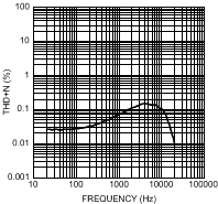
| VDD = 3.6 V | POUT = 600 mW | RL = 4 Ω |
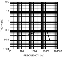
| VDD = 5 V | POUT = 1.2 W | RL = 4 Ω |
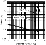
| f = 1 kHz | RL = 4 Ω |
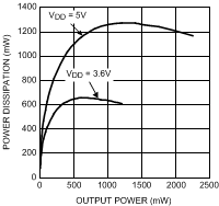
| f = 1 kHz | RL = 4 Ω |
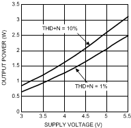
| f = 1 kHz | RL = 4 Ω |
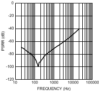
| VDD = 3.6 V | VRIPPLE = 200 mVP-P | RL = 8 Ω |
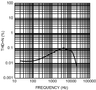
| VDD = 3.6 V | POUT = 400 mW | RL = 8 Ω |
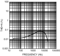
| VDD = 5 V | POUT = 850 mW | RL = 8 Ω |
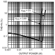
| f = 1 kHz | RL = 8 Ω |
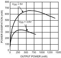
| f = 1 kHz | RL = 8 Ω |
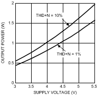
| f = 1 kHz | RL = 8 Ω |