SNVS484H January 2007 – July 2015 LM5001 , LM5001-Q1
PRODUCTION DATA.
- 1 Features
- 2 Applications
- 3 Description
- 4 Revision History
- 5 Pin Configuration and Functions
- 6 Specifications
- 7 Detailed Description
- 8 Applications and Implementation
- 9 Layout
- 10Device and Documentation Support
- 11Mechanical, Packaging, and Orderable Information
Package Options
Mechanical Data (Package|Pins)
- D|8
Thermal pad, mechanical data (Package|Pins)
Orderable Information
1 Features
- AEC-Q100 Qualified (TJ = –40°C to 125°C)
- Integrated 75-V N-Channel MOSFET
- Ultra-Wide Input Voltage Range from
3.1 V to 75 V - Integrated High Voltage Bias Regulator
- Adjustable Output Voltage
- 1.5% Output Voltage Accuracy
- Current Mode Control with Selectable Compensation
- Wide Bandwidth Error Amplifier
- Integrated Current Sensing and Limiting
- Integrated Slope Compensation
- 85% Maximum Duty Cycle Limit
- Single Resistor Oscillator Programming
- Oscillator Synchronization Capability
- Enable / Undervoltage Lockout (UVLO) Pin
- Thermal Shutdown
2 Applications
- DC-DC Power Supplies for Industrial, Communications, and Automotive Applications
- Boost, Flyback, SEPIC and Forward Converter Topologies
3 Description
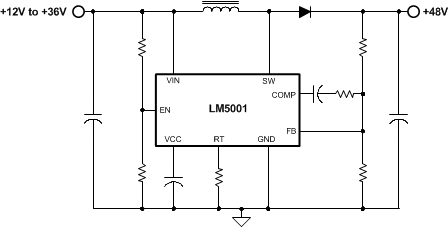
The LM5001 high-voltage switch-mode regulator features all of the functions necessary to implement efficient high-voltage Boost, Flyback, SEPIC and Forward converters, using few external components. This easy-to-use regulator integrates a 75-V NChannel MOSFET with a 1-A peak current limit. Current mode control provides inherently simple loop compensation and line-voltage feed-forward for superior rejection of input transients. The switching frequency is set with a single resistor and is programmable up to 1.5 MHz. The oscillator can also be synchronized to an external clock. Additional protection features include: current limit, thermal shutdown, undervoltage lockout and remote shutdown capability.
Device Information(1)
| DEVICE NAME | PACKAGE | BODY SIZE |
|---|---|---|
| LM5001 | SOIC (8) | 4.9 mm x 3.91 mm |
| WSON (8) | 4 mm x 4 mm | |
| LM5001Q1 | SOIC (8) | 4.9 mm x 3.91 mm |
- For all available packages, see the orderable addendum at the end of the datasheet.
