SNVS961E APRIL 2013 – January 2016 LM5023
PRODUCTION DATA.
- 1 Features
- 2 Applications
- 3 Description
- 4 Revision History
- 5 Pin Configuration and Functions
- 6 Specifications
-
7 Detailed Description
- 7.1 Overview
- 7.2 Functional Block Diagram
- 7.3 Feature Description
- 7.4 Device Functional Modes
- 8 Application and Implementation
- 9 Power Supply Recommendations
- 10Layout
- 11Device and Documentation Support
- 12Mechanical, Packaging, and Orderable Information
Package Options
Mechanical Data (Package|Pins)
- DGK|8
Thermal pad, mechanical data (Package|Pins)
- DGK|8
Orderable Information
7 Detailed Description
7.1 Overview
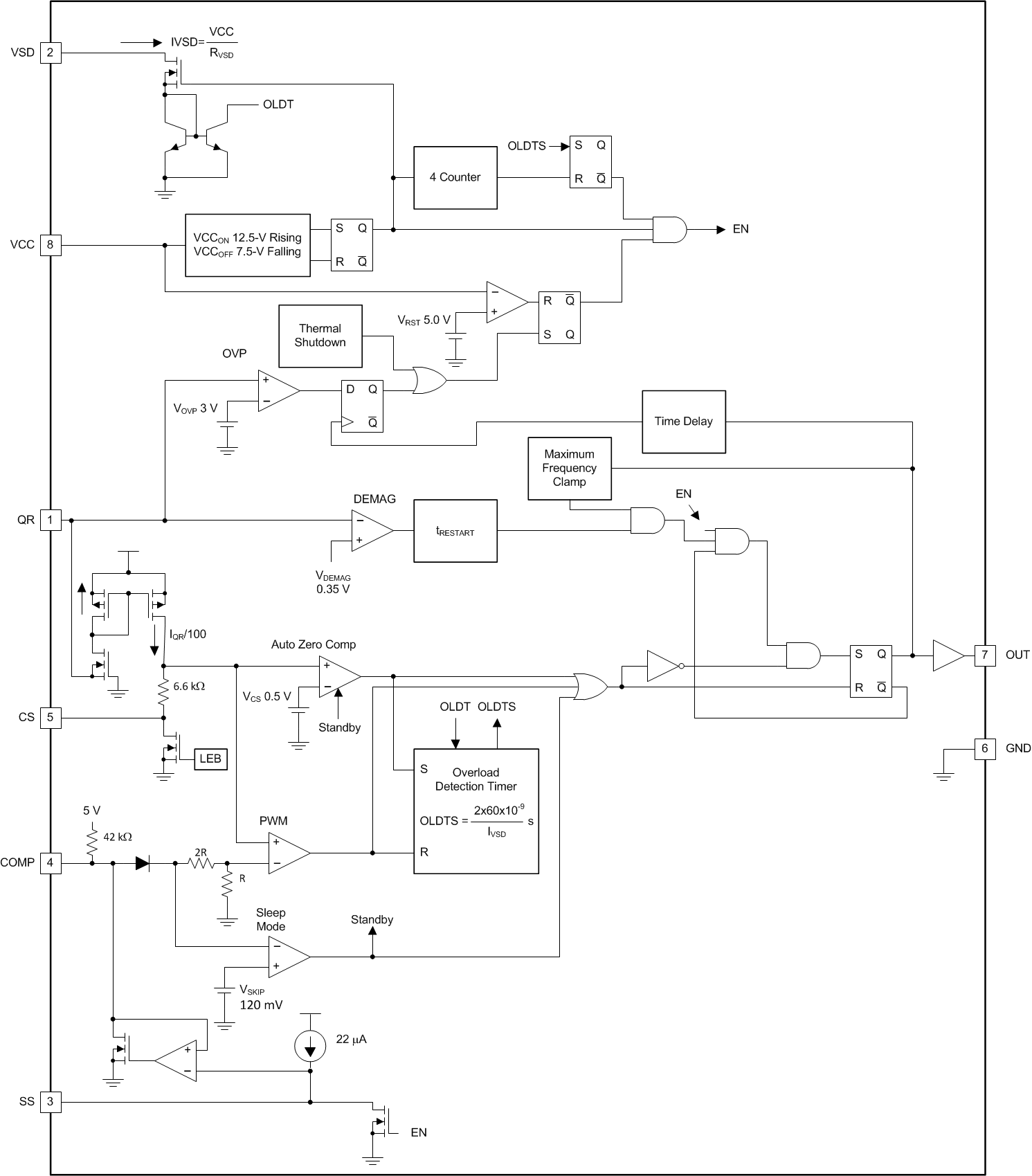
The LM5023 is a quasi-resonant PWM controller which contains all of the features needed to implement a highly efficient off-line power supply. The LM5023 uses the transformer auxiliary winding for demagnetization detection to ensure quasi-resonant operation (valley-switching) to minimize switching losses. For applications that need to meet the ENERGY STAR low standby power requirements, the LM5023 features an extremely low lq current (346 µA) and skip-cycle mode which reduces power consumption at light loads. The LM5023 uses a feedback signal from the output to provide a very accurate output-voltage regulation <1%. To reduce overheating and stress during a sustained overload conditions the LM5023 offers a hiccup mode for over-current protection and provides a current-limit restart timer to disable the outputs and forcing a delayed restart (hiccup mode).
For offline start-up, an external depletion mode N-channel MOSFET can be used. This method is recommended for applications where a very low standby power (<50 mW) is required. For application where a low standby power is not as critical, an enhancement mode, N-channel MOSFET can be used. If an OV is detected on the auxiliary winding (QR pin), the device permanently latches off, requiring recycling of power to restart. VCC voltage must be brought lower than VRST to reset the latch. Additional features include line-current feedforward, pulse-by-pulse current limit, and a maximum frequency clamp of 130 kHz.
7.3 Feature Description
7.3.1 Detailed Pin Description
7.3.1.1 QR Pin
The QR pin is connected to the auxiliary winding voltage divider and valley-switching delay capacitor which are also connected to GND. The auxiliary winding is monitored to detect quasi-resonant operation. The pin is also used to detect an output OV fault, which results in shutdown of the converter. Connect the capacitor and divider low-side resistor with short traces to the QR and GND pins. Avoid high dV/dt traces close to the QR pin connection and net.
7.3.1.2 VSD Pin
The VSD pin is connected to the gate of an external high-voltage start-up MOSFET. The VDS pin controls the gate of the external start-up MOSFET. When the VCC exceeds VCC(on), the VSD pin is pulled low which turns off the start-up MOSFET. Avoid high frequency or high dV/dt traces close to this net.
7.3.1.3 SS Pin
The SS pin is connected to a capacitor selected to control the start-up soft-start time. Place a high quality ceramic capacitor with short traces to SS and GND.
7.3.1.4 COMP Pin
The COMP pin is the input to the pulse width modulator, and skip cycle comparators. There is an internal pull up resistance of 42-kΩ on the COMP pin. Traces from the opto-coupler to the COMP pin should have minimal loop area. It is recommended to shield the COMP trace with ground planes to minimize noise pick up. If a capacitor connects to COMP and GND use short traces.
7.3.1.5 CS Pin
CS is the current sense input for current mode control, and peak current limit. A small ceramic filter capacitor may be placed on CS to GND with short traces, to filter any ringing present during the MOSFET turn on. The current sense resistor current should be returned to the bulk capacitor ground terminal to minimize the primary high current loop area.
7.3.1.6 GND Pin
The GND pin is the signal and power reference for the controller. The GND pin should be connected to the VCC capacitor with a short trace, and be kelvin connected to be the ground reference for components connected to the signal pins.
7.3.1.7 OUT Pin
The OUT pin is connected to the primary MOSFET typically through a small resistance to limit switching speed of the MOSFET. This pin generates high dV/dt signals and should be routed as far away from the signal pins as possible.
7.3.1.8 VCC Pin
The VCC pin must be decoupled to GND with a good quality, low ESR, low ESL ceramic bypass capacitors with short traces to the VCC and GND pins. Additional bulk capacitance may be required to maintain VCC during start-up, but always use a ceramic bypass capacitor as well.
7.3.2 Start-Up
Referring to Figure 8, when the AC rectified line voltage is applied to the bulk-energy-storage capacitor; the N-channel depletion mode MOSFET is turned on and supplies the charging current to the VCC capacitor. When the voltage on the VCC pin reaches 12.5-V typical, the PWM controller, soft-start circuit and gate driver are enabled.
When the LM5023 is enabled and the OUT drive signal starts switching the flyback MOSFET, energy is being stored and then transferred from the transformer primary to the secondary windings. A bias winding, shown in Figure 8, delivers energy to the VCC capacitor to sustain the voltage on the VCC pin. The voltage supplied from the auxiliary winding should be within the range of 10 V to 14 V (where 16 V is the absolute maximum rating).
After reaching the VCCON threshold, the LM5023 VSD open drain output, which is pulled up to VCC during start-up, goes low. This applies a negative gate to source voltage on the depletion mode MOSFET turning it off. This disables the high-voltage start-up circuit. The high-voltage start-up circuit can be implemented in either of two ways; the first is shown in Figure 8, which uses an N-channel depletion modle FET, the second is shown in Figure 9, which uses an N-channel enhancement mode FET. The circuit using the depletion mode FET will have the lowest standby power. The standby power consumption of the FET is the voltage across the start-up FET multiplied by the drain-to-source cutoff current with gate negatively biased, this is typically 0.1 µA.
Standby power of the start-up FET calculation is shown in Equation 1 through Equation 5.


where
- ID(off) is the depletion mode FETs leakage current

When VCC < VCCON the standby current consumption of the IC = ICC(st), nominally 340 µA.
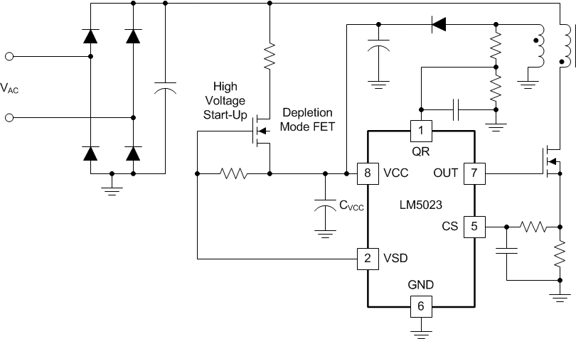 Figure 8. Start-Up With a Depletion Mode FET
An alternative start-up circuit employs an enhancement mode FET with pull-up resistors connected from the rectified DC bus to the gate of the FET, Figure 9. After the input AC power is applied, the enhancement mode FET supplies the charging current to the VCC capacitor CVCC. After reaching the VCCON threshold, the LM5023 VSD open drain output, which is pulled up to VCC during start-up, goes low. This grounds the gate of the start-up MOSFET, turning it off. The start-up resistors are always in the circuit, therefore the standby power consumed will be higher than if a depletion mode FET were used.


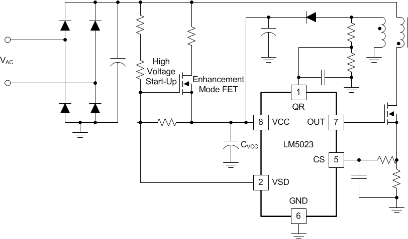 Figure 9. Start-Up With an Enhancement Mode FET
7.3.3 Quasi-Resonant Operation
A quasi-resonant controlled flyback converter operates by storing energy in the transformer's primary during the MOSFET's on-time. During the on-time (tON) VIN is applied across the primary of the transformer. The primary current starts out at zero and ramps towards a peak value (IPEAK). When the peak-primary current reaches the feedback compensation error voltage the PWM comparator resets the output drive, turning off the MOSFET. Due to the phasing of the transformer, the output diode is reverse-biased during the MOSFET on-time.
During the MOSFET's off time the output diode is forward biased and the stored energy in the transformer primary inductor is transferred to the output. The voltage seen on the secondary winding is VOUT plus the output diode's forward voltage drop, VF. The current in the secondary winding linearly decreases from IPEAK × Np/Ns to zero, refer to Figure 11.
When the current in the secondary reaches zero, the transformer is demagnetized, and there is an open circuit on the secondary, and with the primary MOSFET also turned off, there is an open on the primary. A resonant circuit is formed between the transformers primary inductance and the MOSFET output capacitance. The resonant frequency is calculated by Equation 11.

During the resonant period the drain voltage of the MOSFET will ring down towards ground, refer to Figure 10. When the drain voltage is at its minimum the flyback MOSFET is turned back on. The point where the voltage is at its minimum is calculated by Equation 12.

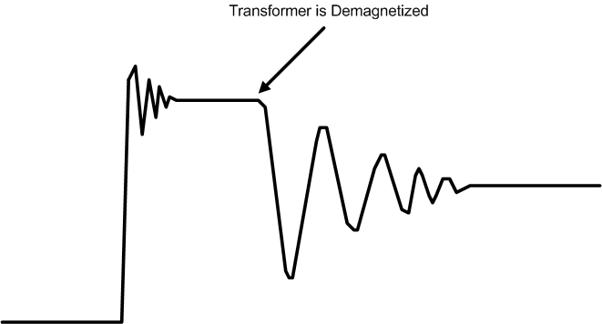 Figure 10. The Flyback Drain Voltage Waveform
Transformer demagnetization is detected by sensing the transformers auxiliary winding. When the transformer is demagnetized the auxiliary winding voltage follows the drain of the MOSFET and changes from VOUT × NAUX/Ns to –VIN × NAUX/Np. Internal to the LM5203 QR pin is a comparator with a 0.35-V reference. As the auxiliary-winding voltage falls below 0.35 V, the voltage is sensed and the comparator sets the PWM flip-flop turning on the flyback MOSFET. Figure 11 shows the QR converter typical waveforms; the auxiliary winding voltage, and primary and secondary current waveforms. It is possible to adjust the delay on the auxiliary winding with a resistor and external capacitor to ensures that the MOSFET switches when its drain voltage is at its minimum. Refer to the schematic in Figure 15 and the section on Valley Switching for details. The benefits of QR operation are reduced EMI, and reduced turn-on switching losses.
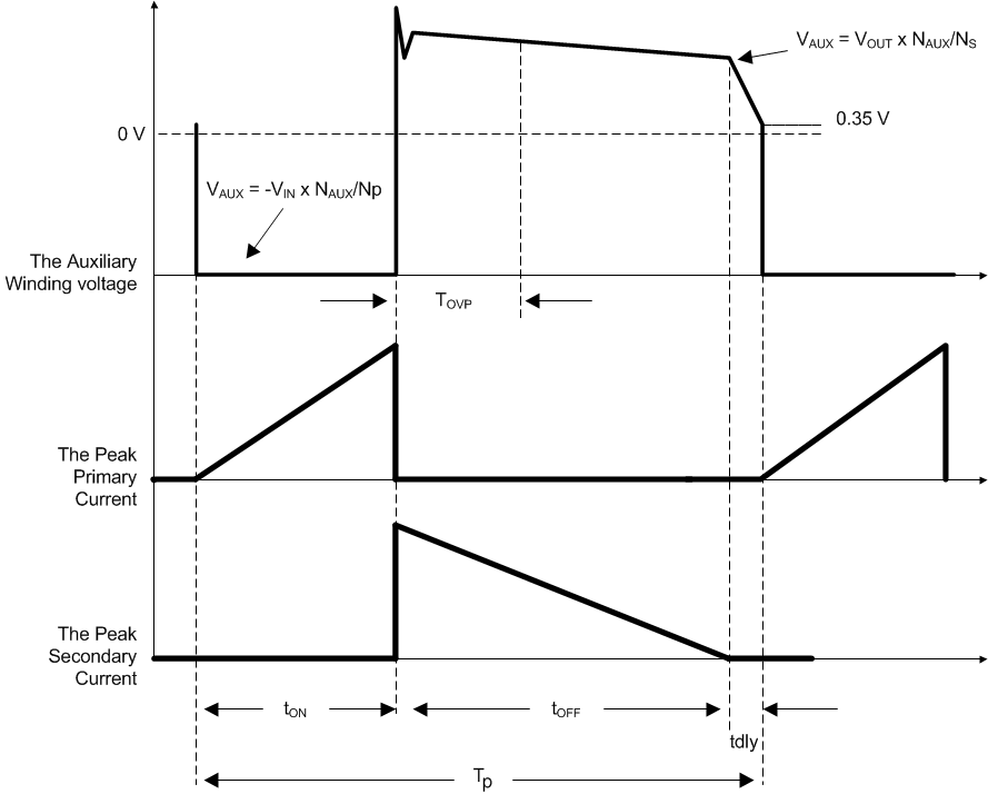 Figure 11. QR Converter Typical Waveforms
7.3.4 Quasi-Resonant Operating Frequency
When the primary-side flyback MOSFET turns on, the current ramps up until the peak-primary current exceeds the feedback compensation error voltage. When this occurs the PWM comparator resets the output drive, turning off the MOSFET. The current ramps up with a slope shown in Equation 13.

The tON time of the switch is calculated by Equation 14.

When the primary-side flyback MOSFET is turned off, the energy stored in the primary inductance is transfer to the secondary inductance, the off time to transfer all of the energy is shown in Equation 15.

where
- NSP = NS/NP
The total switching period is shown in Equation 15.

The resonant circuit created by the transformer primary inductance and the MOSFETs switch node capacitance is the tDLY time, refer to Figure 11.


Equation 19 represents the relationship of switching frequency, LP, and NPS.

The QR flyback converter does not operate at a fixed frequency. The frequency varies with the output load, input line voltage, or a combination of the two. In order to keep LM5023 frequency below the EMI starting limit of 150 kHz per CISPR--22, the LM5023 has an internal timer which prevents the output drive from restarting within 7.69 μs of the previous driver output (OUT) low-to-high transition. This timer clamps the maximum switching frequency at 130 kHz (typical).
7.3.5 PWM Comparator
The PWM comparator compares the current sense signal with the loop error voltage from the COMP pin. The COMP pin voltage is reduced by a fixed 0.75-V offset and then attenuated by a 3:1 resistor divider. The PWM comparator input offset voltage is designed such that less than 0.75 V at the COMP pin will result in a zero duty cycle at the controller output.
7.3.6 Soft-Start
The soft-start feature allows the power converter to gradually reach the initial steady state operating point, thereby reducing start-up stresses and current surges. At power on, after the VCC reaches the VCCON threshold, an internal 22-μA current source charges an external capacitor connected to the SS pin. The capacitor voltage will ramp up slowly and will limit the COMP pin voltage and the duty cycle of the output pulses.
7.3.7 Gate Driver
The LM5023 driver (OUT) was designed to drive the gate of an N-channel MOSFET and is capable of sourcing a peak current of 0.4 A and sinking 0.7 A.
7.3.7.1 Skip-Cycle Operation
During light-load conditions, the efficiency of the switching power supply typically drops as the losses associated with switching and operating bias currents of the converter become a significant percentage of the power delivered to the load. The largest component of the power loss is the switching loss associated with the gate driver and external MOSFET gate charge and the switched-node capacitance energy. Each PWM cycle consumes a finite amount of energy as the MOSFET is turned on and then turned off. These switching losses are proportional to the frequency of operation.
To improve the light-load efficiency the LM5023 enters a skip-cycle mode during light-load conditions. As the output load is decreased, the COMP pin voltage is reduced by the voltage feedback loop to reduce the flyback converters peak-primary current. Referring to the Functional Block Diagram, the PWM comparator input tracks the COMP pin voltage through a 0.75-V level-shift circuit and a 3:1 resistor divider. As the COMP pin voltage falls, the input to the PWM comparator falls proportionately. When the PWM comparator input falls to 120 mV, the skip cycle comparator detects the light-load condition and disables output pulses from the controller. The LM5023 also reduces all internal bias currents, while in skip mode, to further reduce quiescent power. The controller continues to skip switching cycles until the power supply output falls and the COMP pin voltage increases to demand more output current. The number of cycles skipped will depend on the load and the response time of the frequency voltage loop compensation network. Eventually the COMP voltage will increase when the voltage loop requires more current to sustain the regulated output voltage. When the PWM comparator input exceeds 155 mV (30-mV hysteresis), normal fixed-frequency switching resumes. Typical light-load operation power-supply designs will produce a short burst of output pulses followed by a long skip-cycle interval (no drive pulses). The result is a large reduction in the average input power.
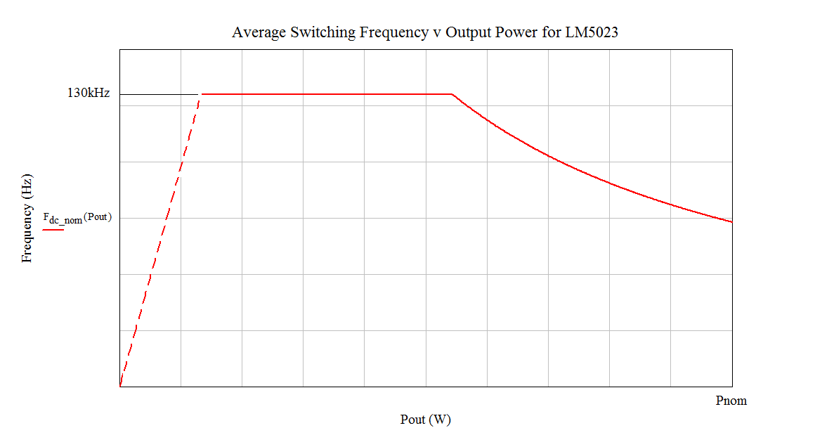 Figure 12. LM5023 Modulation Curve
7.3.8 Current Limit and Current Sense
The LM5023 provides a cycle-by-cycle over current protection feature. Current limit is triggered by an internal current sense comparator with a threshold of 500 mV. If the CS pin voltage plus the current limit feedforward signal voltage exceeds 500 mV, the MOSFET drive signal (OUT) will be terminated. An RC filter, located near the LM5023 CS pin is recommended to attenuate the noise coupled from the power FET’s gate to source switching. The CS pin capacitance is discharged at the end of each PWM cycle by an internal switch. The discharge switch remains on for an additional 130 ns for leading edge blanking (LEB). LEB prevents the LM5023 current sense comparator from being falsely triggered due to the noise generated by the switch currents initial spike. The LM5023 current sense comparator is very fast and may respond to short-duration noise pulses. Layout considerations are critical for the current-sense filter and sense resistor. The capacitor associated with the CS filter must be placed very close to the device and connected directly to the pins of the device (CS and GND). If a current sense transformer is used, both leads of the transformer secondary should be routed to the sense resistor, which should also be located close to the device. If a current sense resistor located in the power FET’s source is used for current sense, a low inductance resistor is required. In this case, all of the noise-sensitive low-current grounds should be connected in common near the device and then a single connection should be made.
7.4 Device Functional Modes
According to the input voltage, the VCC voltage, and the output load conditions, the device can operate in different modes:
- At start-up, when VCC is less than the VCCON threshold, the VSD open drain output is pulled up to VCC which turns on the depletion mode MOSFET. The depletion mode MOSFET charges the VCC capacitor.
- When VCC exceeds the VCCON threshold, the VSC open drain output is pulled to ground which turns off the depletion mode MOSFET, disabling the high-voltage start-up circuit as long as VCC > VCC(off).
- At power on, when VCC reaches the VCCON threshold, the device starts switching to deliver power to the converter output. On initial power up soft-start is initiated by a 22-µA current source that charges a capacitor on the SS pin. The SS pin limits the voltage on the COMP pin voltage and the duty cycle of the OUT pulses.
- Soft-start ends based on the voltage required on the COMP pin to deliver the required power to achieve voltage regulation. Depending on the load condition, the converter operates in normal or skip-cycle mode.
- Normal mode is the full-load to light-load condition where the controller output is enabled every cycle.
- Skip-cycle mode occurs at light to no-load where the controller output is disabled based on the COMP pin voltage. The ICC current is reduced to ICCST when the output is disabled in skip cycle mode.
- The device operation can be stopped by the events listed below:
- If VCC drops below VCCOFF threshold, the device stops switching and the start-up sequence repeats.
- If a fault is detected the driver is latched off until VCC reduces to VCCOFF, and the start-up sequence is initiated.
- If an overload condition exceeds the overload timer duration, the output is turned off until VCC reduces to VCCOFF, and the start-up sequence is initiated.
