SNVS703H February 2011 – November 2014 LM5046
PRODUCTION DATA.
- 1 Features
- 2 Applications
- 3 Description
- 4 Revision History
- 5 Pin Configuration and Functions
- 6 Specifications
-
7 Detailed Description
- 7.1 Overview
- 7.2 Functional Block Diagram
- 7.3
Feature Description
- 7.3.1 High-Voltage Start-Up Regulator
- 7.3.2 Line Undervoltage Detector
- 7.3.3 Overvoltage Protection
- 7.3.4 Reference
- 7.3.5 Oscillator, Sync Input
- 7.3.6 Cycle-by-Cycle Current Limit
- 7.3.7 Hiccup Mode
- 7.3.8 PWM Comparator
- 7.3.9 RAMP Pin
- 7.3.10 Slope Pin
- 7.3.11 Soft-Start
- 7.3.12 Gate Driver Outputs
- 7.3.13 Synchronous Rectifier Control Outputs (SR1 & SR2)
- 7.3.14 Soft-Start of the Synchronous Rectifiers
- 7.3.15 Pre-Bias Startup
- 7.3.16 Soft-Stop
- 7.3.17 Soft-Stop Off
- 7.3.18 Thermal Protection
- 7.4 Device Functional Modes
-
8 Application and Implementation
- 8.1 Application Information
- 8.2
Typical Application
- 8.2.1 Design Requirements
- 8.2.2
Detailed Design Procedure
- 8.2.2.1 Phase-Shifted Full-Bridge Operation
- 8.2.2.2 Control Method Selection
- 8.2.2.3 Voltage Mode Control Using the LM5046
- 8.2.2.4 Current Mode Control Using the LM5046
- 8.2.2.5 VIN and VCC
- 8.2.2.6 For Applications With > 100 V Input
- 8.2.2.7 UVLO and OVP Voltage Divider Selection
- 8.2.2.8 Current Sense
- 8.2.2.9 Hiccup Mode Current Limit Restart
- 8.2.2.10 Augmenting the Gate Drive Strength
- 8.2.3 Application Curve
- 9 Power Supply Recommendations
- 10Layout
- 11Device and Documentation Support
- 12Mechanical, Packaging, and Orderable Information
Package Options
Mechanical Data (Package|Pins)
Thermal pad, mechanical data (Package|Pins)
- PWP|28
Orderable Information
7 Detailed Description
7.1 Overview
The LM5046 PWM controller contains all of the features necessary to implement a Phase-Shifted Full-Bridge (PSFB) topology power converter using either current mode or voltage mode control. This device is intended to operate on the primary side of an isolated dc-dc converter with input voltage up to 100 V. This highly integrated controller-driver provides dual 2A high and low side gate drivers for the four external bridge MOSFETs plus control signals for secondary side synchronous rectifiers. External resistors program the dead-time to enable Zero-Volt Switching (ZVS) of the primary FETs. Please refer to the Application and Implementation section for details on the operation of the PSFB topology. Intelligent startup of synchronous rectifier allows turn-on of the power converter into the pre-bias loads. Cycle-by-cycle current limit protects the power components from load transients while hiccup mode protection limits average power dissipation during extended overload conditions. Additional features include programmable soft-start, soft-start of the synchronous rectifiers, and a 2 MHz capable oscillator with synchronization capability and thermal shutdown.
7.2 Functional Block Diagram
7.3 Feature Description
7.3.1 High-Voltage Start-Up Regulator
The LM5046 contains an internal high voltage start-up regulator that allows the input pin (VIN) to be connected directly to the supply voltage over a wide range from 14 V to 100 V. The input can withstand transients up to 105 V. When the UVLO pin potential is greater than 0.4 V, the VCC regulator is enabled to charge an external capacitor connected to the VCC pin. The VCC regulator provides power to the voltage reference (REF) and the gate drivers (HO1/HO2 and LO1/LO2). When the voltage on the VCC pin exceeds its Under Voltage (UV) threshold, the internal voltage reference (REF) reaches its regulation set point of 5V and the UVLO voltage is greater than 1.25 V, the soft-start capacitor is released and normal operation begins. The regulator output at VCC is internally current limited. The value of the VCC capacitor depends on the total system design, and its start-up characteristics. The recommended range of values for the VCC capacitor is 0.47 μF to 10 µF.
The internal power dissipation of the LM5046 can be reduced by powering VCC from an external supply. The output voltage of the VCC regulator is initially regulated to 9.5 V. After the synchronous rectifiers are engaged (which is approximately when the output voltage in within regulation), the VCC voltage is reduced to 7.7 V. In typical applications, an auxiliary transformer winding is connected through a diode to the VCC pin. This winding must raise the VCC voltage above 8 V to shut off the internal start-up regulator. Powering VCC from an auxiliary winding improves efficiency while reducing the controller’s power dissipation. The VCC UV circuit will still function in this mode, requiring that VCC never falls below its UV threshold during the start-up sequence. The VCC regulator series pass transistor includes a diode between VCC and VIN that should not be forward biased in normal operation. Therefore, the auxiliary VCC voltage should never exceed the VIN voltage.
An external DC bias voltage can be used instead of the internal regulator by connecting the external bias voltage to both the VCC and the VIN pins. This implementation is shown in the Application and Implementation section. The external bias must be greater than 10 V and less than the VCC maximum voltage rating of 14 V.
7.3.2 Line Undervoltage Detector
The LM5046 contains a dual level Under-Voltage Lockout (UVLO) circuit. When the UVLO pin voltage is below 0.4 V, the controller is in a low current shutdown mode. When the UVLO pin voltage is greater than 0.4 V but less than 1.25 V, the controller is in standby mode. In standby mode the VCC and REF bias regulators are active while the controller outputs are disabled. When the VCC and REF outputs exceed their respective under-voltage thresholds and the UVLO pin voltage is greater than 1.25 V, the soft-start capacitor is released and the normal operation begins. An external set-point voltage divider from VIN to GND can be used to set the minimum operating voltage of the converter. The divider must be designed such that the voltage at the UVLO pin will be greater than 1.25 V when VIN enters the desired operating range. UVLO hysteresis is accomplished with an internal 20μA current sink that is switched on or off into the impedance of the set-point divider. When the UVLO threshold is exceeded, the current sink is deactivated to quickly raise the voltage at the UVLO pin. When the UVLO pin voltage falls below the 1.25 V threshold, the current sink is enabled causing the voltage at the UVLO pin to quickly fall. The hysteresis of the 0.4V shutdown comparator is internally fixed at 50 mV.
The UVLO pin can also be used to implement various remote enable / disable functions. Turning off the converter by forcing the UVLO pin to standby condition (0.4 V < UVLO < 1.25 V) provides a controlled soft-stop. Refer to the Soft-Stop section for more details.
7.3.3 Overvoltage Protection
An external voltage divider can be used to set either an over voltage or an over temperature protection. During an OVP condition, the SS and SSSR capacitors are discharged and all the outputs are disabled. The divider must be designed such that the voltage at the OVP pin is greater than 1.25 V when over voltage/temperature condition exists. Hysteresis is accomplished with an internal 20μA current source. When the OVP pin voltage exceeds 1.25 V, the 20 μA current source is activated to quickly raise the voltage at the OVP pin. When the OVP pin voltage falls below the 1.25 V threshold, the current source is deactivated causing the voltage at the OVP to quickly fall. Refer to the Application and Implementation section for more details.
7.3.4 Reference
The REF pin is the output of a 5 V linear regulator that can be used to bias an opto-coupler transistor and external housekeeping circuits. The regulator output is internally current limited to 15mA. The REF pin needs to be locally decoupled with a ceramic capacitor, the recommended range of values are from 0.1 μF to 10 μF
7.3.5 Oscillator, Sync Input
The LM5046 oscillator frequency is set by a resistor connected between the RT pin and AGND. The RT resistor should be located very close to the device. To set a desired oscillator frequency (FOSC), the necessary value of RT resistor can be calculated from Equation 1:

For example, if the desired oscillator frequency is 400 kHz i.e. each phase (LO1 or LO2) at 200 kHz, the value of RT will be 25 kΩ. If the LM5046 is to be synchronized to an external clock, that signal must be coupled into the RT pin through a 100 pF capacitor. The RT pin voltage is nominally regulated at 2.0 V and the external pulse amplitude should lift the pin to between 3.5 V and 5.0 V on the low-to-high transition. The synchronization pulse width should be between 15 and 200 ns. The RT resistor is always required, whether the oscillator is free running or externally synchronized and the SYNC frequency must be equal to, or greater than the frequency set by the RT resistor. When syncing to an external clock, it is recommended to add slope compensation by connecting an appropriate resistor from the VCC pin to the CS pin. Also disable the SLOPE pin by grounding it.
7.3.6 Cycle-by-Cycle Current Limit
The CS pin is to be driven by a signal representative of the transformer’s primary current. If the voltage on the CS pin exceeds 0.75 V, the current sense comparator immediately terminates the PWM cycle. A small RC filter connected to the CS pin and located near the controller is recommended to suppress noise. An internal 18 Ω MOSFET discharges the external current sense filter capacitor at the conclusion of every cycle. The discharge MOSFET remains on for an additional 40 ns after the start of a new PWM cycle to blank leading edge spikes. The current sense comparator is very fast and may respond to short duration noise pulses. Layout is critical for the current sense filter and the sense resistor. The capacitor associated with CS filter must be placed very close to the device and connected directly to the CS and AGND pins. If a current sense transformer is used, both the leads of the transformer secondary should be routed to the filter network, which should be located close to the IC. When designing with a current sense resistor, all of the noise sensitive low power ground connections should be connected together near the AGND pin, and a single connection should be made to the power ground (sense resistor ground point).
7.3.7 Hiccup Mode
The LM5046 provides a current limit restart timer to disable the controller outputs and force a delayed restart (i.e. Hiccup mode) if a current limit condition is repeatedly sensed. The number of cycle-by-cycle current limit events required to trigger the restart is programmed by the external capacitor at the RES pin. During each PWM cycle, the LM5046 either sources or sinks current from the RES capacitor. If current limit is detected, the 5 μA current sink is disabled and a 30 μA current source is enabled. If the RES voltage reaches the 1.0 V threshold, the following restart sequence occurs, as shown in Figure 10:
- The SS and SSSR capacitors are fully discharged
- The 30 μA current source is turned-off and the 10 μA current source is turned-on.
- Once the voltage at the RES pin reaches 4.0V the 10 μA current source is turned-off and a 5 μA current sink is turned-on, ramping the voltage on the RES capacitor down to 2.0 V.
- Once RES capacitor reaches 2.0V, threshold, the 10μA current source is turned-on again. The RES capacitor voltage is ramped between 4.0V and 2.0V eight times.
- When the counter reaches eight, the RES pin voltage is pulled low and the soft-start capacitor is released to begin a soft-start sequence. The SS capacitor voltage slowly increases. When the SS voltage reaches 1.0 V, the PWM comparator will produce the first narrow pulse.
- If the overload condition persists after restart, cycle-by-cycle current limiting will begin to increase the voltage on the RES capacitor again, repeating the hiccup mode sequence.
- If the overload condition no longer exists after restart, the RES pin will be held at ground by the 5 μA current sink and the normal operation resumes.
The hiccup mode function can be completely disabled by connecting the RES pin to the AGND pin. In this configuration the cycle-by-cycle protection will limit the maximum output current indefinitely, no hiccup restart sequences will occur.
 Figure 10. Hiccup Mode Delay and Soft-Start Timing Diagram
7.3.8 PWM Comparator
The LM5046 pulse width modulator (PWM) comparator is a three input device, it compares the signal at the RAMP pin to the loop error signal or the soft-start, whichever is lower, to control the duty cycle. This comparator is optimized for speed in order to achieve minimum controllable duty cycles. The loop error signal is received from the external feedback and isolation circuit in the form of a control current into the COMP pin. The COMP pin current is internally mirrored by a matching pair of NPN transistors which sink current through a 5 kΩ resistor connected to the 5 V reference. The resulting control voltage passes through a 1 V offset, followed by a 2:1 resistor divider before being applied to the PWM comparator.
An opto-coupler detector can be connected between the REF pin and the COMP pin. Because the COMP pin is controlled by a current input, the potential difference across the opto-coupler detector is nearly constant. The bandwidth limiting phase delay which is normally introduced by the significant capacitance of the opto-coupler is thereby greatly reduced. Higher loop bandwidths can be realized since the bandwidth limiting pole associated with the opto-coupler is now at a much higher frequency. The PWM comparator polarity is configured such that with no current flowing into the COMP pin, the controller produces maximum duty cycle.
7.3.9 RAMP Pin
The voltage at the RAMP pin provides the modulation ramp for the PWM comparator. The PWM comparator compares the modulation ramp signal at the RAMP pin to the loop error signal to control the duty cycle. The modulation ramp signal can be implemented either as a ramp proportional to the input voltage, known as feed-forward voltage mode control, or as a ramp proportional to the primary current, known as current mode control. The RAMP pin is reset by an internal MOSFET with an RDS(ON) of 5.5 Ω at the conclusion of each PWM cycle. The ability to configure the RAMP pin for either voltage mode or current mode allows the controller to be implemented for the optimum control method depending upon the design constraints. Refer to the Application and Implementation section for more details on configuring the RAMP pin for feed-forward voltage mode control and peak current mode control.
7.3.10 Slope Pin
For duty cycles greater than 50% (25% for each phase), peak current mode control is subject to sub-harmonic oscillation. Sub-harmonic oscillation is normally characterized by observing alternating wide and narrow duty cycles. This can be eliminated by adding an artificial ramp, known as slope compensation, to the modulating signal at the RAMP pin. The SLOPE pin provides a current source ramping from 0 to 100μA, at the frequency set by the RT resistor, for slope compensation. The ramping current source at the SLOPE pin can be utilized in a couple of different ways to add slope compensation to the RAMP signal:
1) As shown in Figure 11(a), the SLOPE and RAMP pins can be connected together through an appropriate resistor to the CS pin. This configuration will inject current sense signal plus slope compensation to the RAMP pin but CS pin will not see any slope compensation. Therefore, in this scheme slope compensation will not affect the current limit.
2) In a second configuration, as shown in Figure 11(b), the SLOPE, RAMP and CS pins can be tied together. In this configuration the ramping current source from the SLOPE pin will flow through the filter resistor and filter capacitor, therefore both the CS pin and the RAMP pin will see the current sense signal plus the slope compensation ramp. In this scheme, the current limit is compensated by the slope compensation and the current limit onset point will vary.
If slope compensation is not required, for example in feed-forward voltage mode control, the SLOPE pin must be connected to the AGND pin. When the RT pin is synched to an external clock, it is recommended to disable the SLOPE pin and add slope compensation externally by connecting an appropriate resistor from the VCC pin to the CS pin. Please refer to the Application and Implementation section for more details.
7.3.11 Soft-Start
The soft-start circuit allows the power converter to gradually reach a steady state operating point, thereby reducing the start-up stresses and current surges. When bias is supplied to the LM5046, the SS capacitor is discharged by an internal MOSFET. When the UVLO, VCC and REF pins reach their operating thresholds, the SS capacitor is released and is charged with a 20µA current source. Once the SS pin voltage crosses the 1 V offset, SS controls the duty cycle. The PWM comparator is a three input device; it compares the RAMP signal against the lower of the signals between the soft-start and the loop error signal. In a typical isolated application, as the secondary bias is established, the error amplifier on the secondary side soft-starts and establishes closed-loop control, steering the control away from the SS pin.
One method to shutdown the regulator is to ground the SS pin. This forces the internal PWM control signal to ground, reducing the output duty cycle quickly to zero. Releasing the SS pin begins a soft-start cycle and normal operation resumes. A second shutdown method is presented in the UVLO section.
7.3.12 Gate Driver Outputs
The LM5046 provides four gate drivers: two floating high side gate drivers HO1 and HO2 and two ground referenced low side gate drivers LO1 and LO2. Each internal driver is capable of sourcing 1.5A peak and sinking 2A peak. The low-side gate drivers are powered directly by the VCC regulator. The HO1 and HO2 gate drivers are powered from a bootstrap capacitor connected between BST1/BST2 and HS1/HS2 respectively. An external diode connected between VCC (anode pin) and BST (cathode pin) provides the high side gate driver power by charging the bootstrap capacitor from VCC when the corresponding switch node (HS1/HS2 pin) is low. When the high side MOSFET is turned on, BST1 rises to a peak voltage equal to VCC + VHS1 where VHS1 is the switch node voltage.
The BST and VCC capacitors should be placed close to the pins of the LM5046 to minimize voltage transients due to parasitic inductances since the peak current sourced to the MOSFET gates can exceed 1.5A. The recommended value of the BST capacitor is 0.1 μF or greater. A low ESR / ESL capacitor, such as a surface mount ceramic, should be used to prevent voltage droop during the HO transitions.
Figure 12 illustrates the sequence of the LM5046 gate-drive outputs. Initially, the diagonal HO1 and LO2 are turned-on together during the power transfer cycle, followed by the freewheel cycle, where HO1 and HO2 are kept on. In the subsequent phase, the diagonal HO2 and LO1 are turned-on together during the power transfer cycle, followed by a freewheel cycle, where LO1 and LO2 are kept on. The power transfer mode is often called the active mode and the freewheel mode is often called as the passive mode. The dead-time between the passive mode and the active mode, TPA, is set by the RD1 resistor and the dead-time between the active mode and the passive mode, TAP, is set by the RD2 resistor. Refer to the Application and Implementation section for more details on the operation of the phase-shifted full-bridge topology.
If the COMP pin is open circuit, the outputs will operate at maximum duty cycle. The maximum duty cycle for each phase is limited by the dead-time set by the RD1 resistor. If the RD1 resistor is set to zero then the maximum duty cycle is slightly less than 50% due to the internally fixed dead-time. The internally fixed dead-time is 30 ns which does not vary with the operating frequency. The maximum duty cycle for each output can be calculated from Equation 2:
Where, TPA is the time set by the RD1 resistor and FOSC is the frequency of the oscillator. For example, if the oscillator frequency is set at 400 kHz and the TPA time set by the RD1 resistor is 60 ns, the resulting DMAX will be equal to 0.488.
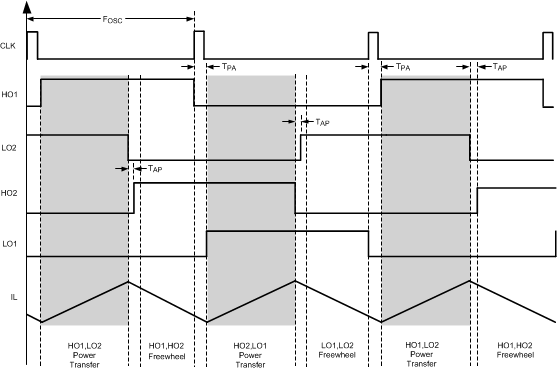 Figure 12. Timing Diagram Illustrating the Sequence of Gate-Driver Outputs in the PSFB Topology
7.3.13 Synchronous Rectifier Control Outputs (SR1 & SR2)
Synchronous rectification (SR) of the transformer secondary provides higher efficiency, especially for low output voltage converters, compared to the diode rectification. The reduction of rectifier forward voltage drop (0.5 V – 1.5 V) to 10 mV – 200 mV VDS voltage for a MOSFET significantly reduces rectification losses. In a typical application, the transformer secondary winding is center tapped, with the output power inductor in series with the center tap. The SR MOSFETs provide the ground path for the energized secondary winding and the inductor current. From Figure 13 it can be seen that when the HO1/LO2 diagonal is turned ON, power transfer is enabled from the primary. During this period, the SR1 MOSFET is enabled and the SR2 MOSFET is turned-off. The secondary winding connected to the SR2 MOSFET drain is twice the voltage of the center tap at this time. At the conclusion of the HO1/LO2 pulse, the inductor current continues to flow through the SR2 MOSFET body diode. Since the body diode causes more loss than the SR MOSFET, efficiency can be improved by minimizing the TSRON period. In the LM5046, the time TSRON is internally fixed to be 30ns. The 30ns internally fixed dead-time, along with inherent system delays due to galvanic isolation, plus the gate drive ICs, will provide sufficient margin to prevent the shoot-through current.
During the freewheeling period, the inductor current flows in both the SR1 and SR2 MOSFETs, which effectively shorts the transformer secondary. The SR MOSFETs are disabled at the rising edge of the CLK, which also disables HO1 or LO1. As shown in Figure 13, SR1 is disabled at the same instant as HO1 is disabled, and SR2 is disabled at the same instant as LO1 is disabled. The dead-times, TSROFF and TPA achieve two different things but are set by single resistor, RD1. Therefore, RD1 value should be selected such that the SR1/SR2 turns-off before the next power transfer cycle is initiated by TPA.
The SR drivers are powered by the REF regulator and each SR output is capable of sourcing 0.1A and sinking 0.4A peak. The amplitude of the SR drivers is limited to 5 V. The 5 V SR signals enable the LM5046 to transfer SR control across the isolation barrier either through a solid-state isolator or a pulse transformer. The actual gate sourcing and sinking currents for the synchronous MOSFETs are provided by the secondary-side bias and gate drivers.
TPA and TAP can be programmed by connecting a resistor between RD1 and RD2 pins and AGND. It should be noted that while RD1 effects the maximum duty cycle, RD2 does not. The RD1 and RD2 resistors should be located very close to the device. The formula for RD1 and RD2 resistors are given in Equation 3:

If the desired dead-time for TPA is 60 ns, then the RD1 will be 20 kΩ.
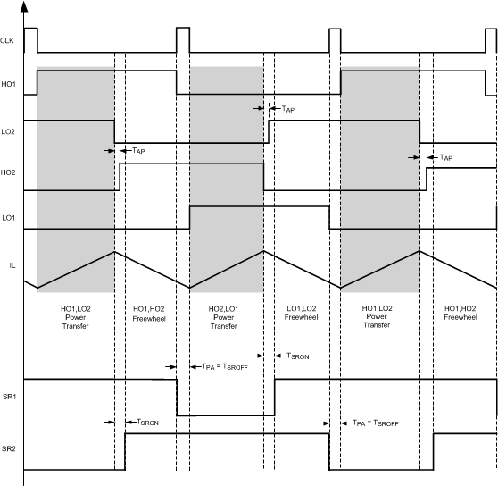 Figure 13. Synchronous Rectifier Timing Diagram
7.3.14 Soft-Start of the Synchronous Rectifiers
In addition to the basic soft-start already described, the LM5046 contains a second soft-start function that gradually turns on the synchronous rectifiers to their steady-state duty cycle. This function keeps the synchronous rectifiers off during the basic soft-start allowing a linear start-up of the output voltage even into pre-biased loads. Then the SR output duty cycle is gradually increased to prevent output voltage disturbances due to the difference in the voltage drop between the body diode and the channel resistance of the synchronous MOSFETs. Initially, when bias is supplied to the LM5046, the SSSR capacitor is discharged by an internal MOSFET. When the SS capacitor reaches a 2 V threshold and once it is established that COMP is in control of the duty cycle i.e. ICOMP < 800 µA, the SSSR discharge is released and SSSR capacitor begins charging with a 20 µA current source. Once the SSSR cap crosses the internal 1 V threshold, the LM5046 begins the soft-start of the synchronous FETs. The SR soft-start follows a leading edge modulation technique, that is, the leading edge of the SR pulse is soft-started as opposed trailing edge modulation of the primary FETs. As shown in Figure 14(a), SR1 and SR2 are turned-on simultaneously with a narrow pulse-width during the freewheeling cycle. At the end of the freewheel cycle i.e. at the rising edge of the internal CLK, the SR FET in-phase with the next power transfer cycle is kept on while the SR FET out of phase with it is turned-off. The in-phase SR FET is kept on throughout the power transfer cycle and at the end of it, both the primary FETs and the in-phase SR FETs are turned-off together. The synchronous rectifier outputs can be disabled by grounding the SSSR pin.
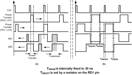 Figure 14. (a) Waveforms during Soft-Start (b) Waveforms after Soft-Start
7.3.15 Pre-Bias Startup
A common requirement for power converters is to have a monotonic output voltage start-up into a pre-biased load i.e. a pre-charged output capacitor. In a pre-biased load condition, if the synchronous rectifiers are engaged prematurely they will sink current from the pre-charged output capacitors resulting in an undesired output voltage dip. This condition is undesirable and could potentially damage the power converter. The LM5046 utilizes unique control circuitry to ensure intelligent turn-on of the synchronous rectifiers such that the output has a monotonic startup. Initially, the SSSR capacitor is held at ground to disable the synchronous MOSFETs allowing the body diode to conduct. The synchronous rectifier soft-start is initiated once it is established the duty cycle is controlled by the COMP instead of the soft-start capacitor i.e. ICOMP < 800 µA and the voltage at the SS pin > 2 V. The SSSR capacitor is then released and is charged by a 20 µA current source. Further, as shown in Figure 15, a 1 V offset on the SSSR pin is used to provide additional delay. This delay ensures the output voltage is in regulation avoiding any reverse current when the synchronous MOSFETs are engaged.
7.3.16 Soft-Stop
As shown in Figure 16, if the UVLO pin voltage falls below the 1.25 V standby threshold, but above the 0.4 V shutdown threshold, the SSSR capacitor is soft-stopped with a 60 µA current source (3 times the charging current). Once the SSSR pin reaches the 1.0 V threshold, both the SS and SSSR pins are immediately discharged to GND. Soft-stopping the power converter gradually winds down the energy in the output capacitors and results in a monotonic decay of the output voltage. During the hiccup mode, the same sequence is executed except that the SSSR is discharged with a 120 µA current source (6 times the charging current). In case of an OVP, VCC UV, thermal limit or a VREF UV condition, the power converter hard-stops, whereby all of the control outputs are driven to a low state immediately.
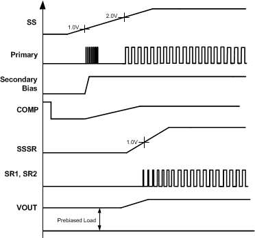 Figure 15. Pre-Bias Voltage Startup Waveforms
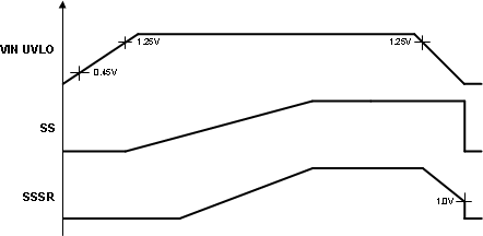 Figure 16. Stop-Stop Waveforms during a UVLO Event
7.3.17 Soft-Stop Off
The Soft-Start Off (SSOFF) pin gives additional flexibility by allowing the power converter to be configured for hard-stop during line UVLO and hiccup mode condition. If the SS OFF pin is pulled up to the 5 V REF pin, the power converter hard-stops in any fault condition. Hard-stop drives each control output to a low state immediately. Refer to Table 1 for more details.
Table 1. Soft-Stop in Fault Conditions
| FAULT CONDITION | SSSR |
|---|---|
| UVLO (UVLO<1.25V) |
Soft-Stop 3x the charging rate |
| OVP (OVP>1.25V) |
Hard-Stop |
| Hiccup (CS>0.75 and RES>1V) |
Soft-Stop 6x the charging rate |
| VCC/VREF UV | Hard-Stop |
| Internal Thermal Limit | Hard-Stop |
Note: All the above conditions are valid with SSOFF pin tied to GND. If SSOFF = 5 V, the LM5046 hard-stops in all the conditions. The SS pin remains high in all the conditions until the SSSR pin reaches 1 V.
7.3.18 Thermal Protection
Internal thermal shutdown circuitry is provided to protect the integrated circuit in the event the maximum rated junction temperature is exceeded. When activated, typically at 160°C, the controller is forced into a shutdown state with the output drivers, the bias regulators (VCC and REF) disabled. This helps to prevent catastrophic failures from accidental device overheating. During thermal shutdown, the SS and SSSR capacitors are fully discharged and the controller follows a normal start-up sequence after the junction temperature falls to the operating level (140°C).
7.4 Device Functional Modes
7.4.1 Control Method Selection
The LM5045 is a versatile PWM control IC that can be configured for either current mode control or voltage mode control. The choice of the control method usually depends upon the designer preference. The following must be taken into consideration while selecting the control method. Current mode control can inherently balance flux in both phases of the full-bridge topology. The full-bridge topology, like other double ended topologies, is susceptible to the transformer core saturation. Any asymmetry in the volt-second product applied between the two alternating phases results in flux imbalance that causes a dc buildup in the transformer. This continual dc buildup may eventually push the transformer into saturation. The volt-second asymmetry can be corrected by employing current mode control. In current mode control, a signal representative of the primary current is compared against an error signal to control the duty cycle. In steady-state, this results in each phase being terminated at the same peak current by adjusting the pulse-width and thus applying equal volt-seconds to both the phases.
Current mode control can be susceptible to noise and sub-harmonic oscillation, while voltage mode control employs a larger ramp for PWM and is usually less susceptible. Voltage-mode control with input line feed-forward also has excellent line transient response. When configuring for voltage mode control, a dc blocking capacitor can be placed in series with the primary winding of the power transformer to avoid any flux imbalance that may cause transformer core saturation.
7.4.2 Voltage Mode Control Using the LM5045
To configure the LM5045 for voltage mode control, an external resistor (RFF) and capacitor (CFF) connected to VIN, AGND, and the RAMP pins is required to create a saw-tooth modulation ramp signal shown in Figure 17. The slope of the signal at RAMP will vary in proportion to the input line voltage. The varying slope provides line feed-forward information necessary to improve line transient response with voltage mode control. With a constant error signal, the on-time (TON) varies inversely with the input voltage (VIN) to stabilize the Volt- Second product of the transformer primary. Using a line feed-forward ramp for PWM control requires very little change in the voltage regulation loop to compensate for changes in input voltage, as compared to a fixed slope oscillator ramp. Furthermore, voltage mode control is less susceptible to noise and does not require leading edge filtering. Therefore, it is a good choice for wide input range power converters. Voltage mode control requires a Type-III compensation network, due to the complex-conjugate poles of the L-C output filter.
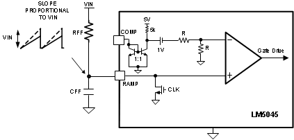 Figure 17. Feed-Forward Voltage Mode Configuration
The recommended capacitor value range for CFF is from 100 pF to 1800 pF. Referring to Figure 17, it can be seen that CFF value must be small enough to be discharged with in the clock pulse-width which is typically within 50ns. The RDS(ON) of the internal discharge FET is 5.5 Ω.
The value of RFF required can be calculated from
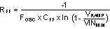
For example, assuming a VRAMP of 1.5 V (a good compromise of signal range and noise immunity), at VINMIN of 36 V (oscillator frequency of 400 kHz and CFF = 470 pF results in a value for RFF of 125 kΩ.
7.4.3 Current Mode Control Using the LM5045
The LM5045 can be configured for current mode control by applying a signal proportional to the primary current to the RAMP pin. One way to achieve this is shown in Figure 18. The primary current can be sensed using a current transformer or sense resistor, the resulting signal is filtered and applied to the RAMP pin through a resistor used for slope compensation. It can be seen that the signal applied to the RAMP pin consists of the primary current information from the CS pin plus an additional ramp for slope compensation, added by the resistor RSLOPE.
The current sense resistor is selected such that during over current condition, the voltage across the current sense resistor is above the minimum CS threshold of 728 mV.
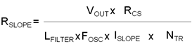
In general, the amount of slope compensation required to avoid sub-harmonic oscillation is equal to at least one-half the down-slope of the output inductor current, transformed to the primary. To mitigate sub-harmonic oscillation after one switching period, the slope compensation has to be equal to one times the down slope of the filter inductor current transposed to primary. This is known as deadbeat control. The slope compensation resistor required to implement dead-beat control can be calculated as follows:
where
- NTR is the turns-ratio with respect to the secondary
For example, for a 3.3 V output converter with a turns-ratio between primary and secondary of 9:1, an output filter inductance (LFILTER) of 800 nH and a current sense resistor (RSENSE) of 150 mΩ, RSLOPE of 1.67 kΩ will suffice.
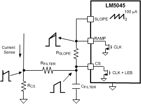 Figure 18. Current Mode Configuration