SNVS234C September 2004 – September 2016 LM5112 , LM5112-Q1
PRODUCTION DATA.
- 1 Features
- 2 Applications
- 3 Description
- 4 Revision History
- 5 Pin Configuration and Functions
- 6 Specifications
- 7 Detailed Description
- 8 Application and Implementation
- 9 Power Supply Recommendations
- 10Layout
- 11Device and Documentation Support
- 12Mechanical, Packaging, and Orderable Information
Package Options
Refer to the PDF data sheet for device specific package drawings
Mechanical Data (Package|Pins)
- NGG|6
Thermal pad, mechanical data (Package|Pins)
Orderable Information
7 Detailed Description
7.1 Overview
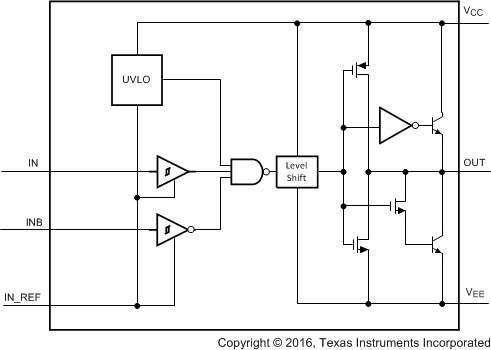
The LM5112 device is a high-speed, high-peak current (7 A) single-channel MOSFET driver. The high-peak output current of the LM5112 device switches power MOSFETs on and off with short rise and fall times, thereby reducing switching losses considerably. The LM5112 device includes both inverting and non-inverting inputs that give the user flexibility to drive the MOSFET with either active low or active high logic signals. The driver output stage consists of a compound structure with MOS and bipolar transistor operating in parallel to optimize current capability over a wide output voltage and operating temperature range. The bipolar device provides high peak current at the critical Miller plateau region of the MOSFET VGS, while the MOS device provides rail-to-rail output swing. The totem pole output drives the MOSFET gate between the gate drive supply voltage VCC and the power ground potential at the VEE pin.
7.2 Functional Block Diagram
 Figure 11. LM5112 Functional Block Diagram
7.3 Feature Description
The control inputs of the driver are high impedance CMOS buffers with TTL compatible threshold voltages. The negative supply of the input buffer is connected to the input ground pin IN_REF. An internal level shifting circuit connects the logic input buffers to the totem pole output drivers. The level shift circuit and the separate input or output ground pins provide the option of single supply or split supply configurations. When driving the MOSFET gate from a single positive supply, the IN_REF and VEE pins are both connected to the power ground.
The isolated input and output stage grounds provide the capability to drive the MOSFET to a negative VGS voltage for a more robust and reliable off state. In split supply configuration, the IN_REF pin is connected to the ground of the controller which drives the LM5112 inputs. The VEE pin is connected to a negative bias supply that can range from the IN_REF potential to as low as 14 V below the VCC gate drive supply. For reliable operation, the maximum voltage difference between VCC and IN_REF or between VCC and VEE is 14 V.
The minimum recommended operating voltage between VCC and IN_REF is 3.5 V. An undervoltage lockout (UVLO) circuit is included in the LM5112 which senses the voltage difference between VCC and the input ground pin, IN_REF. When the VCC to IN_REF voltage difference falls below 2.8 V the driver is disabled and the output pin is held in the low state. The UVLO hysteresis prevents chattering during brown-out conditions; the driver resumes normal operation when the VCC to IN_REF differential voltage exceeds 3 V.
7.4 Device Functional Modes
The device output state is dependent on states of the IN and INB pins. Table 1 lists the output states for different input pin combinations.
Table 1. Device Logic Table
| IN PIN | INB PIN | OUT PIN |
|---|---|---|
| L | L | L |
| L | H | L |
| H | L | H |
| H | H | L |
7.4.1 Inverting Mode
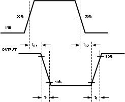
During the inverting mode of operation, INB is used as the control input and the polarity of OUT is reversed with respect to INB. Figure 12 shows a timing diagram of this mode. The IN pin is not used in this mode of operation and must be pulled up to VCC.
 Figure 12. Inverting
7.4.2 Non-Inverting Mode
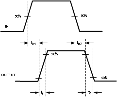
During the non-inverting mode of operation, IN is used as the control input and the polarity of OUT is the same with respect to IN. Figure 13 shows a timing diagram of this mode. The INB pin is not used in this mode of operation and must be connected to IN_REF.
 Figure 13. Non-Inverting