SNVS234C September 2004 – September 2016 LM5112 , LM5112-Q1
PRODUCTION DATA.
- 1 Features
- 2 Applications
- 3 Description
- 4 Revision History
- 5 Pin Configuration and Functions
- 6 Specifications
- 7 Detailed Description
- 8 Application and Implementation
- 9 Power Supply Recommendations
- 10Layout
- 11Device and Documentation Support
- 12Mechanical, Packaging, and Orderable Information
Package Options
Refer to the PDF data sheet for device specific package drawings
Mechanical Data (Package|Pins)
- NGG|6
- DGN|8
Thermal pad, mechanical data (Package|Pins)
Orderable Information
8 Application and Implementation
NOTE
Information in the following applications sections is not part of the TI component specification, and TI does not warrant its accuracy or completeness. TI’s customers are responsible for determining suitability of components for their purposes. Customers should validate and test their design implementation to confirm system functionality.
8.1 Application Information
A leading application for gate drivers such as the LM5112 is providing a high power buffer stage between the PWM output of a control IC and the gates of the primary power switching devices. In other cases, the driver IC is used to drive the power device gates through a drive transformer. Driver ICs are used when it is not feasible to have the primary PWM regulator IC directly drive the switching devices for one or more reasons. The PWM IC may not have the brute drive capability required for the intended switching MOSFET, limiting the switching performance in the application.
The LM5112 is used to drive a low side MOSFET with low switching losses. Either one of the control input pins, IN or INB, are used to control the gate drive to the MOSFET. The choice of the control input pin used depends on the polarity of operation.
8.2 Typical Application
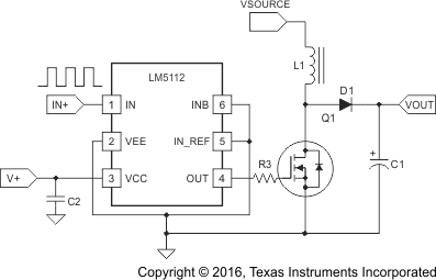
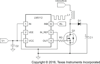
Typical application diagrams for the LM5112 device are shown below, illustrating use in non-inverting and inverting driver configurations. The high peak gate drive current of the LM5112 allows for short rise and fall times on the low-side MOSFET, thereby improving overall efficiency of the system and reducing switching losses.
 Figure 14. Typical Application Diagram (Using Non-Inverting Control Input)
 Figure 15. Typical Application Diagram (Using Inverting Control Input)
8.2.1 Design Requirements
When selecting the proper gate driver device for an end application, some design considerations must be evaluated first to make the most appropriate selection. Among these considerations are input-to-output configuration, the input threshold type, bias supply voltage levels, peak source and sink currents, capacitive load, and switching frequency. Table 2 shows some sample values for a typical application.
Table 2. Design Parameters
| PARAMETER | VALUE |
|---|---|
| Input-to-output logic | Non-inverting |
| VCC bias supply voltage (measured with respect to VEE) |
12 V |
| Supply configuration | Split supply |
| Peak source current | 3 A |
| Peak sink current | 7 A |
| Output load (MOSFET gate capacitance) | 2 nF |
| Gate drive resistor | 1 Ω |
| Switching frequency | 300 kHz |
8.2.2 Detailed Design Procedure
See Power Supply Recommendations, Layout, and Thermal Considerations for key design considerations regarding the input supply, grounding, and thermal calculations specific to the LM5112.
8.2.3 Application Curves
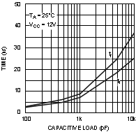
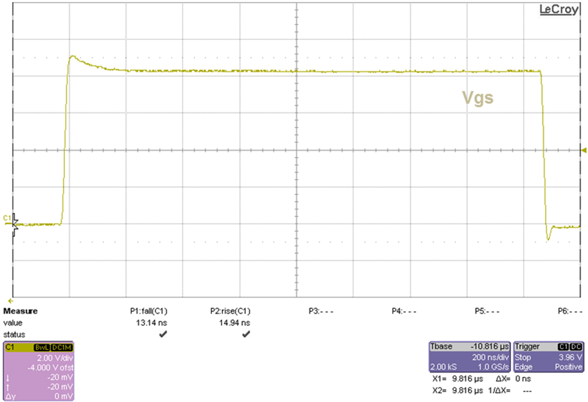
The rise and fall times of the OUT signal depends on the capacitance of the MOSFET gate. Therefore, an appropriate MOSFET must be selected to meet the switching speed and efficiency requirements of the system. Figure 16 shows the rise and fall time curves as a function of capacitive load. Figure 17 shows output rise and fall time measured on an application board, showing actual device performance. The testing conditions for this figure are Cload= 2.2 nF, Rdrive = 1 Ω, and fs = 300 kHz.

