SNVSA67B December 2016 – June 2017 LM5166
PRODUCTION DATA.
- 1 Features
- 2 Applications
- 3 Description
- 4 Revision History
- 5 Pin Configuration and Functions
- 6 Specifications
-
7 Detailed Description
- 7.1 Overview
- 7.2 Functional Block Diagram
- 7.3
Feature Description
- 7.3.1 Integrated Power MOSFETs
- 7.3.2 Selectable PFM or COT Mode Converter Operation
- 7.3.3 Low Dropout Operation and 100% Duty Cycle Mode
- 7.3.4 Adjustable Output Voltage (FB)
- 7.3.5 Adjustable Current Limit
- 7.3.6 Precision Enable (EN) and Hysteresis (HYS)
- 7.3.7 Power Good (PGOOD)
- 7.3.8 Configurable Soft Start (SS)
- 7.3.9 Short-Circuit Operation
- 7.3.10 Thermal Shutdown
- 7.4 Device Functional Modes
-
8 Applications and Implementation
- 8.1 Application Information
- 8.2
Typical Applications
- 8.2.1
Design 1: Wide VIN, Low IQ, High-Efficiency COT Converter Rated at 5 V, 500 mA
- 8.2.1.1 Design Requirements
- 8.2.1.2
Detailed Design Procedure
- 8.2.1.2.1 Custom Design With WEBENCH® Tools
- 8.2.1.2.2 Feedback Resistors - RFB1, RFB2
- 8.2.1.2.3 Switching Frequency - RT
- 8.2.1.2.4 Filter Inductance - LF
- 8.2.1.2.5 Output Capacitors - COUT
- 8.2.1.2.6 Ripple Generation Network - RESR, CFF
- 8.2.1.2.7 Input Capacitor - CIN
- 8.2.1.2.8 Soft-Start Capacitor - CSS
- 8.2.1.2.9 Application Curves
- 8.2.2 Design 2: Wide VIN, Low IQ COT Converter Rated at 3.3 V, 500 mA
- 8.2.3 Design 3: High-Density PFM Converter Rated at 3.3 V, 0.3 A
- 8.2.4 Design 4: Wide VIN, Low IQ PFM Converter Rated at 5 V, 500 mA
- 8.2.5
Design 5: 12-V, 300-mA COT Converter Operating From 24-V or 48-V Input
- 8.2.5.1 Design Requirements
- 8.2.5.2
Detailed Design Procedure
- 8.2.5.2.1 Peak Current Limit Setting - RILIM
- 8.2.5.2.2 Switching Frequency - RRT
- 8.2.5.2.3 Inductor - LF
- 8.2.5.2.4 Input and Output Capacitors - CIN, COUT
- 8.2.5.2.5 Feedback Resistors - RFB1, RFB2
- 8.2.5.2.6 Ripple Generation Network - RA, CA, CB
- 8.2.5.2.7 Undervoltage Lockout Setpoint - RUV1, RUV2, RHYS
- 8.2.5.2.8 Soft Start - CSS
- 8.2.5.3 Application Curves
- 8.2.1
Design 1: Wide VIN, Low IQ, High-Efficiency COT Converter Rated at 5 V, 500 mA
- 9 Power Supply Recommendations
- 10Layout
- 11Device and Documentation Support
- 12Mechanical, Packaging, and Orderable Information
Package Options
Mechanical Data (Package|Pins)
- DRC|10
Thermal pad, mechanical data (Package|Pins)
- DRC|10
Orderable Information
8 Applications and Implementation
NOTE
Information in the following applications sections is not part of the TI component specification, and TI does not warrant its accuracy or completeness. TI’s customers are responsible for determining suitability of components for their purposes. Customers should validate and test their design implementation to confirm system functionality.
8.1 Application Information
The LM5166 only requires a few external components to convert from a wide range of supply voltages to a fixed output voltage. To expedite and streamline the process of designing a LM5166-based converter, a comprehensive LM5166 Quickstart Calculator is available for download to assist the designer with component selection for a given application. WEBENCH® online software is also available to generate complete designs, leveraging iterative design procedures and access to comprehensive component databases. The following sections discuss the design procedure for both COT and PFM converters using specific circuit design examples.
The LM5166 integrates several optional features to meet system design requirements, including precision enable, UVLO, programmable soft start, programmable switching frequency in COT mode, adjustable current limit, and PGOOD indicator. Each application incorporates these features as needed for a more comprehensive design. The application circuits detailed below show LM5166 configuration options suitable for several application use cases. Please see the LM5166EVM-C50A and LM5166EVM-C33A EVM user's guides for more detail.
8.2 Typical Applications
 |
For step-by-step design procedure, circuit schematics, bill of materials, PCB files, simulation and test results of an LM5166-powered implementation, refer to 24-V AC Power Stage with Wide VIN Converter and Battery Gauge for Smart Thermostat reference design. |
8.2.1 Design 1: Wide VIN, Low IQ, High-Efficiency COT Converter Rated at 5 V, 500 mA
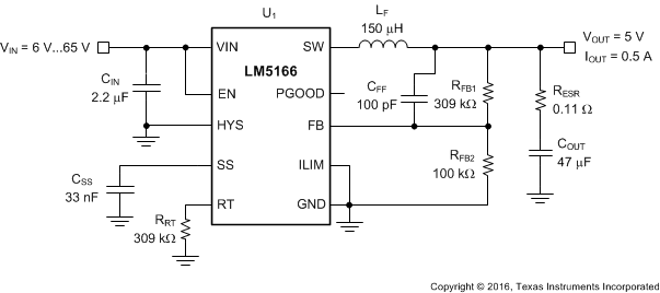 Figure 52. Schematic for Design 1 With VIN(nom) = 24 V, VOUT = 5 V, IOUT(max) = 500 mA, FSW(nom) = 100 kHz
8.2.1.1 Design Requirements
The target efficiency is 90% for loads above 10 mA based on a nominal input voltage of 24 V and an output voltage of 5 V. The required input voltage range is 6 V to 65 V. The LM5166 is chosen to deliver a 5-V output voltage. The switching frequency is set at 100 kHz. The output voltage soft-start time is 4 ms. The required components are listed in Table 4.
Table 4. List of Components for Design 1(1)
| COUNT | REF DES | DESCRIPTION | PART NUMBER | MFR |
|---|---|---|---|---|
| 1 | CIN | Capacitor, Ceramic, 2.2 μF, 100 V, X7R, 10%, 1210 | GRM32ER72A225KA35L | Murata |
| 1 | COUT | Capacitor, Ceramic, 47 μF, 10 V, X7R, 10%, 1210 | GRM32ER71A476KE15L | Murata |
| 1 | CSS | Capacitor, Ceramic, 33 nF, 16 V, X7R, 10%, 0402 | Std | Std |
| 1 | CFF | Capacitor, Ceramic, 100 pF, 50 V, X7R, 10%, 0402 | Std | Std |
| 1 | LF | Inductor, 150 µH, 0.240 Ω typ, 1.4 A Isat, 5 mm max | 7447714151 | Würth |
| Inductor, 150 µH, 0.285 Ω typ, 1.12 A Isat, 5.1 mm max | CDRH105RNP-151NC | Sumida | ||
| 1 | RRT | Resistor, Chip, 309 kΩ, 1/16W, 1%, 0402 | Std | Std |
| 1 | RFB1 | Resistor, Chip, 309 kΩ, 1/16W, 1%, 0402 | Std | Std |
| 1 | RESR | Resistor, Chip, 0.11 Ω, 1/16W, 1%, 0402 | Std | Std |
| 1 | RFB2 | Resistor, Chip, 100 kΩ, 1/16W, 1%, 0402 | Std | Std |
| 1 | U1 | LM5166, Synchronous Buck Converter, VSON-10, ADJ | LM5166DRCR | TI |
8.2.1.2 Detailed Design Procedure
8.2.1.2.1 Custom Design With WEBENCH® Tools
Click here to create a custom design using the LM5166 device with the WEBENCH® Power Designer.
- Start by entering the input voltage (VIN), output voltage (VOUT), and output current (IOUT) requirements.
- Optimize the design for key parameters such as efficiency, footprint, and cost using the optimizer dial.
- Compare the generated design with other possible solutions from Texas Instruments.
The WEBENCH Power Designer provides a customized schematic along with a list of materials with real-time pricing and component availability.
In most cases, these actions are available:
- Run electrical simulations to see important waveforms and circuit performance
- Run thermal simulations to understand board thermal performance
- Export customized schematic and layout into popular CAD formats
- Print PDF reports for the design, and share the design with colleagues
Get more information about WEBENCH tools at www.ti.com/WEBENCH.
8.2.1.2.2 Feedback Resistors – RFB1, RFB2
While the 5-V fixed output version of the LM5166 is suitable here, the adjustable version is chosen to provide the user with the option to trim or margin the output voltage if needed. The feedback resistor divider network comprises the upper feedback resistor RFB1 and lower feedback resistor RFB2. Select RFB1 of 309 kΩ to minimize quiescent current and improve light-load efficiency in this application. With the desired output voltage setpoint of 5 V and VFB = 1.223 V, calculate the resistance of RFB2 using Equation 15 as 100.1 kΩ. Choose the closest available standard value of 100 kΩ for RFB2. See Adjustable Output Voltage (FB) for more details.
8.2.1.2.3 Switching Frequency – RT
The switching frequency of a COT-configured LM5166 is set by the on-time programming resistor at the RT pin. Using Equation 4, a standard 1% resistor of 309 kΩ gives a switching frequency of 92 kHz. Including the inductor RDCR and RDSON2 in the calculation of tOFF (Equation 3) gives an adjusted FSW of 101 kHz at 500 mA. The LM5166 Quickstart Calculator estimates and plots the switching frequency as a function of load current.
Note that at very low duty cycles, the minimum controllable on-time of the high-side MOSFET, TON(min), of 180 ns may affect choice of switching frequency. In CCM, TON(min) limits the voltage conversion step-down ratio for a given switching frequency. The minimum controllable duty cycle is given by Equation 19.

Given a fixed TON(min), it follows that higher switching frequency implies a larger minimum controllable duty cycle. Ultimately, the choice of switching frequency for a given output voltage affects the available input voltage range, solution size, and efficiency. The maximum supply voltage for a given TON(min) before switching frequency reduction occurs is given by Equation 20.

8.2.1.2.4 Filter Inductance – LF
The inductor ripple current (assuming CCM operation) and peak inductor current are given respectively by Equation 21 and Equation 22.


For most applications, choose the inductance such that the inductor ripple current, ΔIL, is between 30% and 60% of the rated load current at nominal input voltage. Calculate the inductance using Equation 23.

Choosing a 150-μH inductor in this design results in 295-mA peak-to-peak ripple current at nominal input voltage of 24 V, equivalent to 59% of the 500-mA rated load current. The peak inductor current at maximum input voltage of 65 V is 675 mA, which is sufficiently below the LM5166 peak current limit of 750 mA.
Check the inductor datasheet to ensure that the inductor saturation current is well above the current limit setting of a particular design. Ferrite designs have low core loss and are preferred at high switching frequencies, so design goals can then concentrate on copper loss and preventing saturation. However, ferrite core materials exhibit a hard saturation characteristic – the inductance collapses abruptly when the saturation current is exceeded. This results in an abrupt increase in inductor ripple current, higher output voltage ripple, not to mention reduced efficiency and compromised reliability. Note that inductor saturation current generally decreases as the core temperature increases.
8.2.1.2.5 Output Capacitors – COUT
Select the output capacitor to limit the capacitive voltage ripple at the converter output. This is the sinusoidal ripple voltage that arises from the triangular ripple current flowing in the capacitor. Select an output capacitance using Equation 24 to limit the capacitive voltage ripple component to 0.5% of the output voltage.

Substituting ΔIL(nom) of 295 mA and ΔVOUT of 25 mV gives COUT greater than 16 μF. Mindful of the voltage coefficient of ceramic capacitors, select a 47-μF, 10-V capacitor with a high-quality dielectric.
8.2.1.2.6 Ripple Generation Network – RESR, CFF
For this design, the Type 2 ripple generation method is selected as it offers a good balance between cost and output voltage ripple. For other methods, see Ripple Generation Methods.
Select a series resistor, RESR, such that sufficient ripple in phase with the inductor current ripple appears at the feedback node, FB, using Equation 7 and Equation 8. Select a feedforward capacitor, CFF, using Equation 9.
With ΔIL(nom) of 295 mA at the nominal input voltage of 24 V, the required RESR is 0.11 Ω. The required feedforward capacitance, CFF, is 100 pF. Calculate the total output voltage ripple in CCM using Equation 25.

8.2.1.2.7 Input Capacitor – CIN
An input capacitor is necessary to limit the input ripple voltage while providing switching-frequency AC current to the buck power stage. To minimize the parasitic inductance in the switching loop, position the input capacitors as close as possible to the VIN and GND pins of the LM5166. The input capacitors conduct a trapezoidal-wave current of peak-to-peak amplitude equal to the output current. It follows that the resultant capacitive component of AC ripple voltage is a triangular waveform. Together with the ESR-related ripple component, the peak-to-peak input ripple voltage amplitude is given by Equation 26.

The input capacitance required for a particular load current, based on an input voltage ripple specification of ΔVIN, is given by Equation 27.

The recommended high-frequency input capacitance is 2.2 μF or higher and should be a high-quality ceramic component with sufficient voltage rating. Based on the voltage coefficient of ceramic capacitors, choose a voltage rating of twice the maximum input voltage. Additionally, some bulk capacitance is required if the LM5166 circuit is not located within approximately 5 cm from the input voltage source. This capacitor provides damping to the resonance associated with parasitic inductance of the supply lines and high-Q ceramics.
8.2.1.2.8 Soft-Start Capacitor – CSS
Connect an external soft-start capacitor for a specific soft-start time. In this example, select a soft-start capacitance of 33 nF based on Equation 18 to achieve a soft-start time of 4 ms.
8.2.1.2.9 Application Curves
Unless otherwise stated, application performance curves were taken at TA = 25°C.
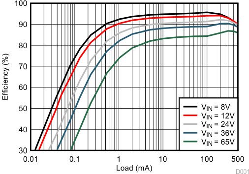
| LF = 150 µH COUT = 47 µF |
FSW(nom) = 100 kHz RRT = 309 kΩ |
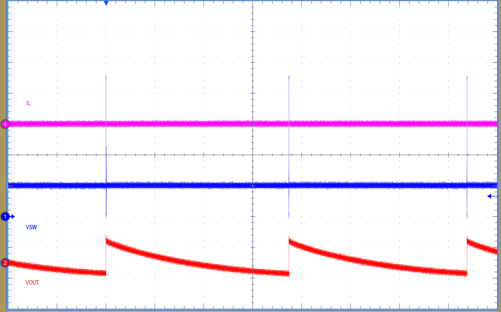
| Time Scale: 20 ms/Div CH1: VSW, 5 V/Div |
CH2: VOUT, 50 mV/Div CH4: IL, 200 mA/Div |
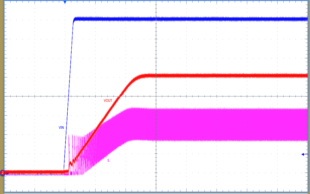
| Time Scale: 2 ms/Div CH1: VIN, 3 V/Div |
CH2: VOUT, 1 V/Div CH4: IL, 200 mA/Div |
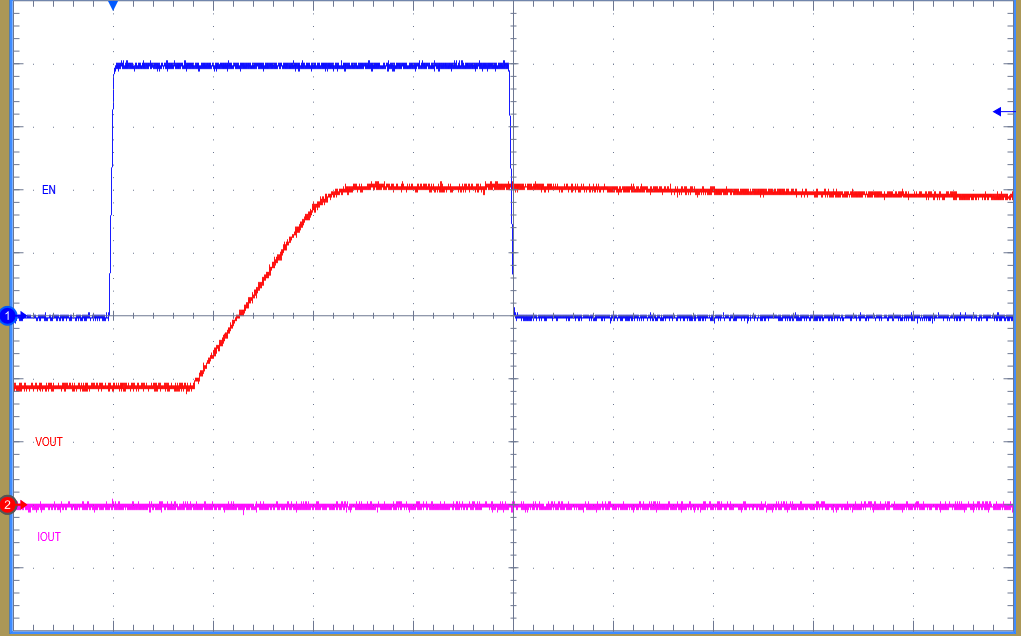
| Time Scale: 2 ms/Div CH1: VEN, 1 V/Div |
CH2: VOUT, 1 V/Div CH4: IOUT, 200 mA/Div |
VIN = 24 V, No Load
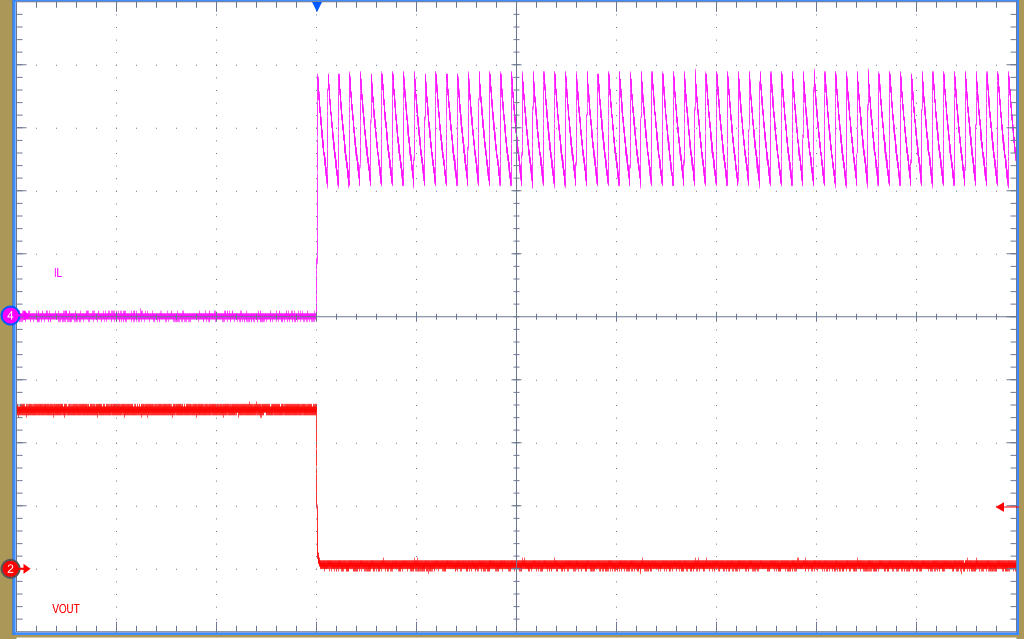
| Time Scale: 1 ms/Div | CH2: VOUT, 2 V/Div CH4: IL, 200 mA/Div |
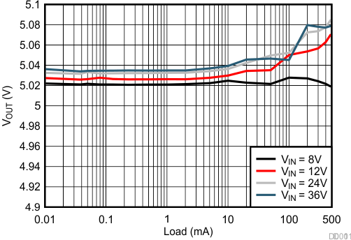
| LF = 150 µH COUT = 47 µF |
FSW(nom) = 100 kHz RRT = 309 kΩ |
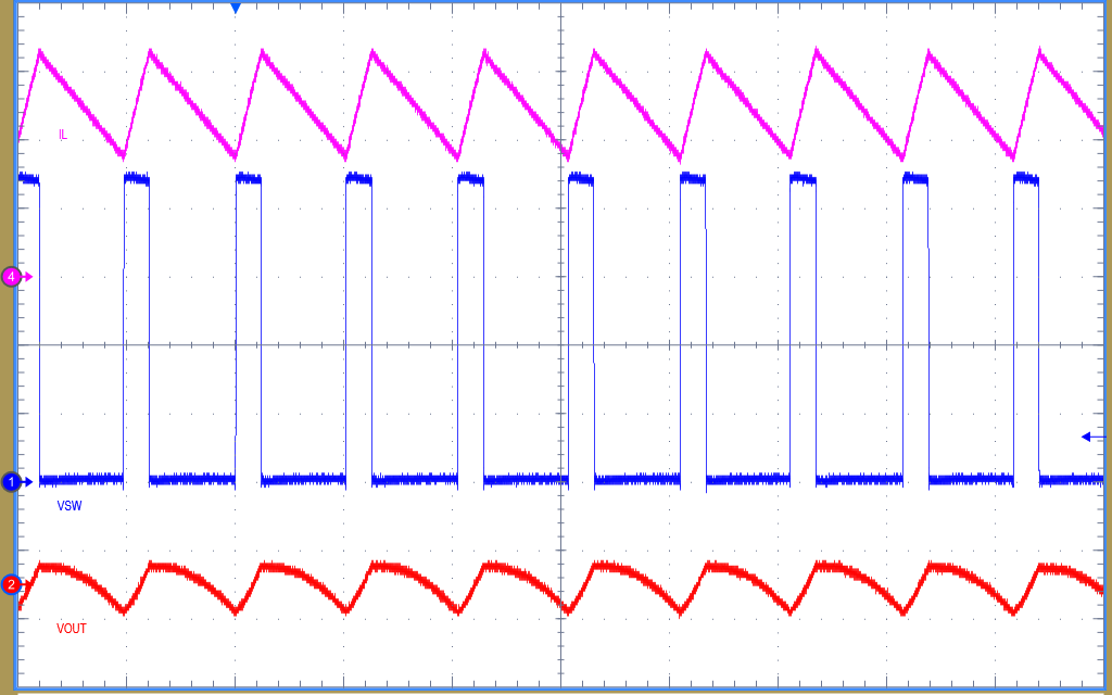
| Time Scale: 10 µs/Div CH1: VSW, 5 V/Div |
CH2: VOUT, 50 mV/Div CH4: IL, 200 mA/Div |
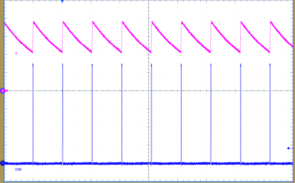
| Time Scale: 100 µs/Div CH1: VSW, 4 V/Div |
CH4: IL, 200 mA/Div |
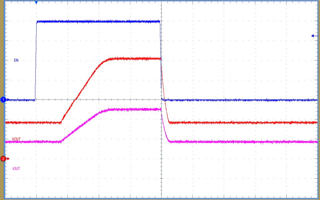
| Time Scale: 2 ms/Div CH1: VEN, 5 V/Div |
CH2: VOUT, 1 V/Div CH4: IOUT, 200 mA/Div |
VIN = 24 V, 500 mA Load
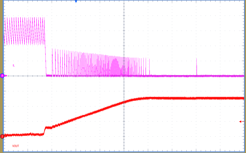
| Time Scale: 1 ms/Div | CH2: VOUT, 2 V/Div CH4: IL, 200 mA/Div |
8.2.2 Design 2: Wide VIN, Low IQ COT Converter Rated at 3.3 V, 500 mA
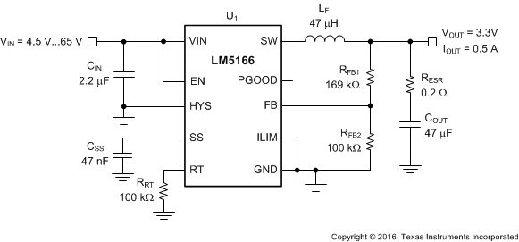 Figure 63. Schematic for Design 2 With VIN(nom) = 12 V, VOUT = 3.3 V, IOUT(max) = 500 mA, FSW(nom) = 200 kHz
8.2.2.1 Design Requirements
The target efficiency is 85% for loads above 10 mA based on a nominal input voltage of 12 V and an output voltage of 3.3 V. The required input voltage range is 4.5 V to 65 V. The LM5166 is chosen to deliver a 3.3-V output voltage. The switching frequency is set at 200 kHz. The output voltage soft-start time is 4 ms. The required components are listed in Table 5.
Table 5. List of Components for Design 2(1)
| COUNT | REF DES | DESCRIPTION | PART NUMBER | MFR |
|---|---|---|---|---|
| 1 | CIN | Capacitor, Ceramic, 2.2 μF, 100 V, X7R, 10%, 1210 | GRM32ER72A225KA35L | Murata |
| 1 | COUT | Capacitor, Ceramic, 47 μF, 10 V, X7R, 10%, 1210 | GRM32ER71A476KE15L | Murata |
| 1 | CSS | Capacitor, Ceramic, 47 nF, 16 V, X7R, 10%, 0402 | Std | Std |
| 1 | LF | Inductor, 47 µH, 0.245 Ω max, 1.2 A Isat, 3.5 mm max | LPS6235-473MR | Coilcraft |
| Inductor, 47 µH, 0.315 Ω typ, 1.3 A Isat, 2.8 mm max | 74404063470 | Würth | ||
| 1 | RRT | Resistor, Chip, 100 kΩ, 1/16W, 1%, 0402 | Std | Std |
| 1 | RFB1 | Resistor, Chip, 169 kΩ, 1/16W, 1%, 0402 | Std | Std |
| 1 | RESR | Resistor, Chip, 0.2 Ω, 1/16W, 1%, 0402 | Std | Std |
| 1 | RFB2 | Resistor, Chip, 100 kΩ, 1/16W, 1%, 0402 | Std | Std |
| 1 | U1 | LM5166, Synchronous Buck Converter, VSON-10, ADJ | LM5166DRCR | TI |
8.2.2.2 Detailed Design Procedure
8.2.2.2.1 Feedback Resistors – RFB1, RFB2
The output voltage of the LM5166 is externally adjustable using a resistor divider network. The divider network comprises the upper feedback resistor RFB1 and lower feedback resistor RFB2. Select RFB1 of 169 kΩ to minimize quiescent current and improve light-load efficiency in this application. With the desired output voltage setpoint of 3.3 V and VFB = 1.223 V, calculate the resistance of RFB2 using Equation 15 as 100.1 kΩ. Choose the closest available standard value of 100 kΩ for RFB2. See Adjustable Output Voltage (FB) for more detail.
8.2.2.2.2 Switching Frequency – RT
The switching frequency of a COT-configured LM5166 is set by the on-time programming resistor at the RT pin. Using Equation 4, a standard 1% resistor of 100 kΩ gives a switching frequency of 190 kHz. Including the inductor RDCR and RDSON2 in the calculation of tOFF (Equation 3) gives an adjusted FSW of 215 kHz at 500 mA. The LM5166 Quick-Start Design Tool estimates and plots the switching frequency as a function of load current.
Note that at very low duty cycles, the minimum controllable on-time of the high-side MOSFET, TON(min), of 180 ns may affect choice of switching frequency. In CCM, TON(min) limits the voltage conversion step-down ratio for a given switching frequency. The minimum controllable duty cycle is given by Equation 19.
Given a fixed TON(min), it follows that higher switching frequency implies a larger minimum controllable duty cycle. Ultimately, the choice of switching frequency for a given output voltage affects the available input voltage range, solution size, and efficiency. The maximum supply voltage for a given TON(min) before switching frequency reduction occurs is given by Equation 20.
8.2.2.2.3 Filter Inductance – LF
The inductor ripple current (assuming CCM operation) and peak inductor current are given respectively by Equation 21 and Equation 22. For most applications, choose an inductance such that the inductor ripple current, ΔIL, is between 30% and 60% of the rated load current at nominal input voltage. Calculate the inductance using Equation 23.
Choosing a 47-μH inductor in this design results in 275-mA peak-to-peak ripple current at nominal input voltage of 12 V, equivalent to 55% of the 500-mA rated load current. The peak inductor current at maximum input voltage of 65 V is 694 mA, which is sufficiently below the LM5166 peak current limit of 750 mA.
8.2.2.2.4 Output Capacitors – COUT
Select the output capacitor to limit the capacitive voltage ripple at the converter output. This is the sinusoidal ripple voltage that arises from the triangular ripple current flowing in the capacitor. Select an output capacitance using Equation 24 to limit the capacitive voltage ripple component to 0.5% of the output voltage.
Substituting ΔIL(nom) of 275 mA and ΔVOUT of 25 mV gives COUT greater than 11 μF. Mindful of the voltage coefficient of ceramic capacitors, select a 47-μF, 10-V capacitor with a high-quality dielectric.
8.2.2.2.5 Ripple Generation Network – RESR
For this design, the Type 1 ripple generation method is selected as it only requires a single external component. For other schemes, see Ripple Generation Methods.
Select a series resistor, RESR, using Equation 5 and Equation 6 such that sufficient ripple in phase with the SW node voltage appears at the feedback node, FB. With ΔIL(nom) of 275 mA at the nominal input voltage of 12 V, the required RESR is 0.2 Ω. Calculate the total output voltage ripple in CCM using Equation 25.
8.2.2.2.6 Input Capacitor – CIN
An input capacitor is necessary to limit the input ripple voltage while providing switching-frequency AC current to the buck power stage. To minimize the parasitic inductance in the switching loop, position the input capacitors as close as possible to the VIN and GND pins of the LM5166. The input capacitors conduct a trapezoidal-wave current of peak-to-peak amplitude equal to the output current. It follows that the resultant capacitive component of AC ripple voltage is a triangular waveform. Together with the ESR-related ripple component, the peak-to-peak input ripple voltage amplitude is given by Equation 26. The input capacitance required for a particular load current, based on an input voltage ripple specification of ΔVIN, is given by Equation 27.
The recommended high-frequency capacitance is 2.2 μF or higher and should be a high-quality ceramic with sufficient voltage rating. Based on the voltage coefficient of ceramic capacitors, choose a voltage rating of twice the maximum input voltage. Additionally, some bulk capacitance is required if the LM5166 circuit is not located within approximately 5 cm from the input voltage source. This capacitor provides damping to the resonance associated with parasitic inductance of the supply lines and high-Q ceramics.
8.2.2.2.7 Soft-Start Capacitor – CSS
Connect an external soft-start capacitor for a specific soft-start time. In this example, select a soft-start capacitance of 47 nF based on Equation 18 to achieve a soft-start time of 6 ms.
8.2.2.2.8 Application Curves
Unless otherwise stated, application curves were taken at TA = 25°C.
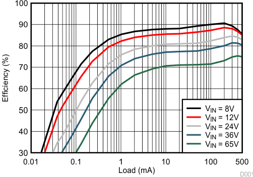
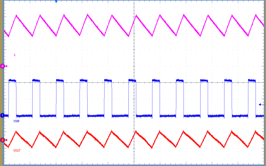
| LF = 47 µH COUT = 47 µF |
FSW(nom) = 200 kHz RRT = 100 kΩ |
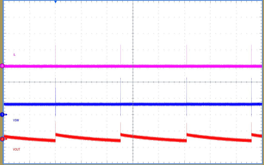
| Time Scale: 20 ms/Div CH1: VSW, 5 V/Div |
CH2: VOUT, 50 mV/Div CH4: IL, 200 mA/Div |
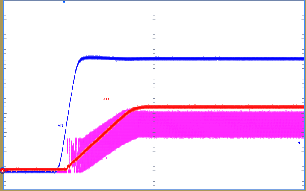
| Time Scale: 2 ms/Div CH1: VIN, 2 V/Div |
CH2: VOUT, 1 V/Div CH4: IL, 200 mA/Div |
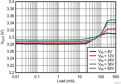
| LF = 47 µH COUT = 47 µF |
FSW(nom) = 200 kHz RRT = 100 kΩ |
| Time Scale: 5 µs/Div CH1: VSW, 5 V/Div |
CH2: VOUT, 50 mV/Div CH4: IL, 200 mA/Div |
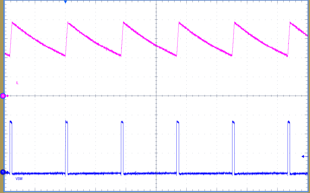
| Time Scale: 100 µs/Div CH1: VSW, 4 V/Div |
CH4: IL, 200 mA/Div |
8.2.3 Design 3: High-Density PFM Converter Rated at 3.3 V, 0.3 A
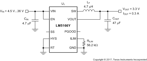 Figure 70. Schematic for Design 3 With VIN(nom) = 24 V, VOUT = 3.3 V, IOUT(max) = 0.3 A, FSW(nom) = 600 kHz
8.2.3.1 Design Requirements
The target efficiency is 75% for loads above 10 mA based on a nominal input voltage of 24 V, an output voltage of 3.3 V, with the emphasis on small solution size. The required input voltage range is 4.5 V to 36 V. The LM5166 has an internally-set soft-start time of 900 µs and an adjustable peak current limit threshold. The required components are listed in Table 6.
Table 6. List of Components for Design 3(1)
| COUNT | REF DES | DESCRIPTION | PART NUMBER | MFR |
|---|---|---|---|---|
| 1 | CIN | Capacitor, Ceramic, 4.7 μF, 50 V, X7R, 10%, 1206 | GRM31CR71H475MA12L | Murata |
| 885012208094 | Würth | |||
| 1 | COUT | Capacitor, Ceramic, 47 μF, 6.3 V, X5R, 10%, 1206 | GRM31CR60J476KE19 | Murata |
| 1 | LF | Inductor, 4.7 µH, 0.18 Ω typ, 2.2 A Isat, 1.2 mm max | TFM252012ALMA4R7TMAA | TDK |
| Inductor, 4.7 µH, 0.3 Ω typ, 2.1 A Isat, 1.2 mm max | Würth | Würth | ||
| 1 | RILIM | Resistor, Chip, 56.2 kΩ, 1/16W, 1%, 0402 | Std | Std |
| 1 | U1 | LM5166Y, Synchronous Buck Converter, VSON-10, 3.3-V Fixed | LM5166YDRCR | TI |
8.2.3.2 Detailed Design Procedure
8.2.3.2.1 Peak Current Limit Setting – RILIM
Install a 56.2-kΩ resistor from ILIM to GND to select a 750-mA peak current limit threshold setting to meet the rated output current of 300 mA in PFM. See Adjustable Current Limit for more detail.
8.2.3.2.2 Switching Frequency – LF
Tie RT to GND to select PFM mode of operation. The inductor, input voltage, output voltage and peak current determine the pulse switching frequency of a PFM-configured LM5166. For a given input voltage, output voltage and peak current, the inductance of LF sets the switching frequency when the output is in regulation. Use Equation 28 to select an inductance of 4.7 μH based on the target PFM converter switching frequency of 600 kHz at 24-V input.

IPK(PFM) in this example is the peak current limit setting of 750 mA plus the inductor current overshoot resulting from the 80-ns peak current comparator delay, tILIM_delay. An additional constraint on the inductance is the 180-ns minimum on-time of the high-side MOSFET. Therefore, to keep the inductor current well controlled, choose an inductance that is larger than LF(min) using Equation 29 where VIN(max) is the maximum input supply voltage for the application, tILIM_delay is 80 ns, tON(min) is 180 ns, the maximum current limit threshold, ILIM(max), is 825 mA, and the maximum allowed peak inductor current, IL(max), is 1.6 A.

Choose an inductor with saturation current rating above the peak current limit setting, and allow for derating of the saturation current at the highest expected operating temperature.
8.2.3.2.3 Output Capacitors – COUT
The output capacitor, COUT, filters the inductor’s ripple current and stores energy to meet the load current requirement when the LM5166 is in sleep mode. The output ripple has a base component of amplitude VOUT/123 related to the typical feedback comparator hysteresis in PFM. The wake-up time from sleep to active mode adds a ripple voltage component that is a function of the output current. Approximate the total output ripple by Equation 30.

Also, the output capacitance must be large enough to accept the energy stored in the inductor without a large deviation in output voltage. Setting this voltage change equal to 1% of the output voltage results in a COUT requirement defined with Equation 31.

In general, select the capacitance of COUT to limit the output voltage ripple at full load current, ensuring that it is rated for worst-case RMS ripple current given by IRMS = IPK(PFM)/2. In this design example, select a 47-μF, 6.3-V capacitor with a high-quality dielectric.
8.2.3.2.4 Input Capacitor – CIN
The input capacitor, CIN, filters the triangular current waveform of the high-side MOSFET (see Figure 89). To prevent large ripple voltage, use a low-ESR ceramic input capacitor sized for the worst-case RMS ripple current given by IRMS = IOUT/2. In this design example, choose a 2.2-μF, 50-V ceramic input capacitor with a high-quality dielectric.
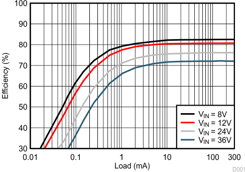
8.2.3.2.5 Application Curves
Unless otherwise stated, application curves were taken at TA = 25°C.
| LF = 4.7 µH COUT = 47 µF |
FSW(nom) = 600 kHz RRT = 0 Ω |
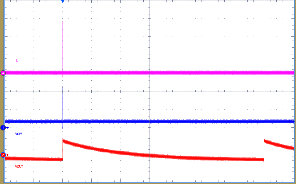
| Time Scale: 20 ms/Div CH1: VSW, 10 V/Div |
CH2: VOUT, 50 mV/Div CH4: IL, 400 mA/Div |
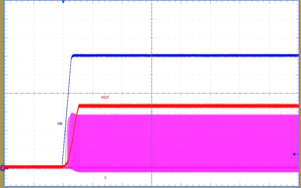
| Time Scale: 2 ms/Div CH1: VIN, 4 V/Div |
CH2: VOUT, 1 V/Div CH4: IL, 400 mA/Div |
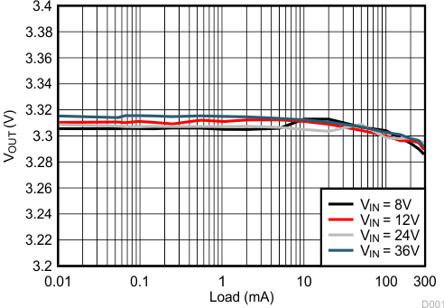
| LF = 4.7 µH COUT = 47 µF |
FSW(nom) = 600 kHz RRT = 0 Ω |
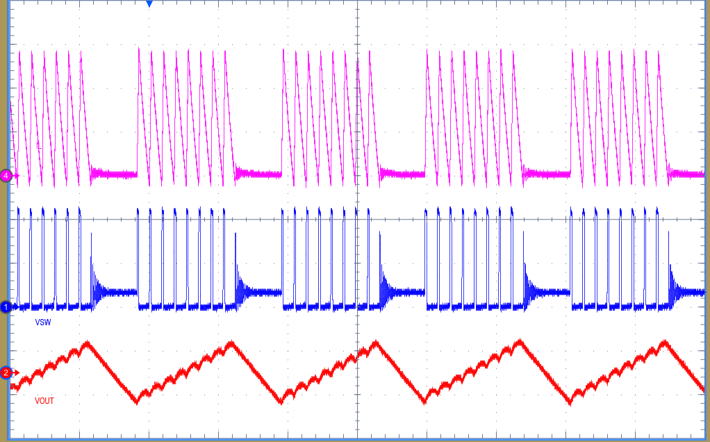
| Time Scale: 10 µs/Div CH1: VSW, 10 V/Div |
CH2: VOUT, 50 mV/Div CH4: IL, 400 mA/Div |
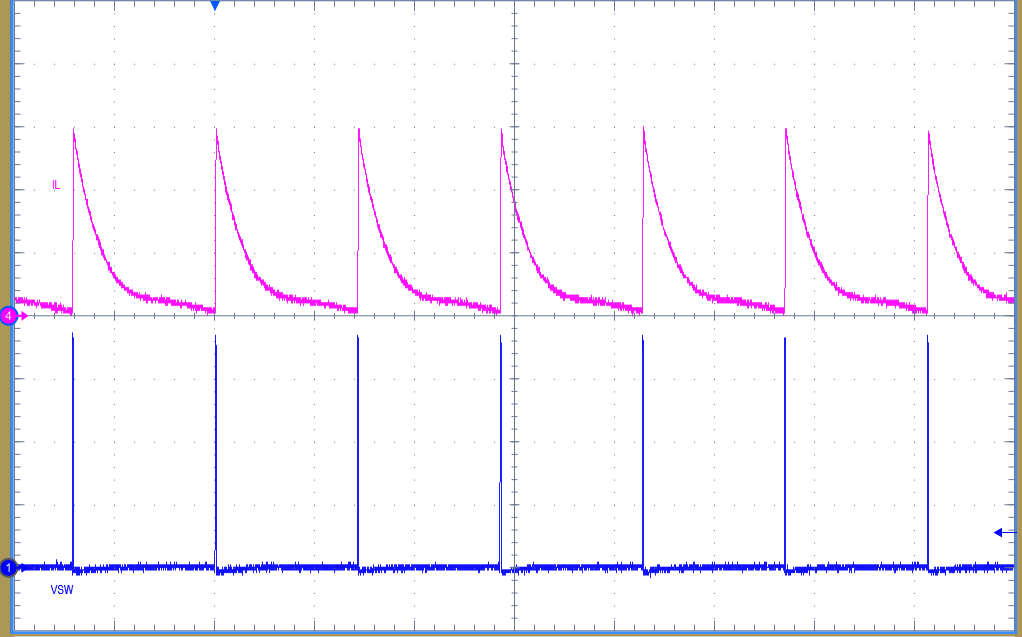
| Time Scale: 20 µs/Div CH1: VSW, 6 V/Div |
CH4: IL, 400 mA/Div |
8.2.4 Design 4: Wide VIN, Low IQ PFM Converter Rated at 5 V, 500 mA
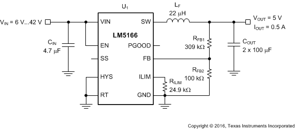 Figure 77. Schematic for Design 4 With VIN(nom) = 12 V, VOUT = 5 V, IOUT(max) = 500 mA, FSW(nom) = 100 kHz
8.2.4.1 Design Requirements
The target efficiency is 85% for loads above 1 mA based on a nominal input voltage of 12 V, an output voltage of 5 V. The required input voltage range is 6 V to 42 V. The LM5166 has an internally-set soft-start time of 900 µs and an adjustable peak current limit threshold. The required components are listed in Table 7.
Table 7. List of Components for Design 4(1)
| COUNT | REF DES | DESCRIPTION | PART NUMBER | MFR |
|---|---|---|---|---|
| 1 | CIN | Capacitor, Ceramic, 4.7 μF, 50 V, X7R, 20%, 1206 | GRM31CR71H475MA12L | Murata |
| C3216X7R1H475M160AC | TDK | |||
| 2 | COUT | Capacitor, Ceramic, 100 μF, 10 V, X5R, 10%, 1210 | GRM32ER61A107ME20K | Murata |
| 1 | LF | Inductor, 22 µH, 0.145 Ω max, 1.7 A Isat, 3.5 mm max | LPS6235-223MR | Coilcraft |
| Inductor, 22 µH, 0.2 Ω max, 2.3 A Isat, 3 mm max | CMLB063T-220MS | Cyntec | ||
| 1 | RILIM | Resistor, Chip, 24.9 kΩ, 1/16W, 1%, 0402 | Std | Std |
| 1 | RFB1 | Resistor, Chip, 309 kΩ, 1/16W, 1%, 0402 | Std | Std |
| 1 | RFB2 | Resistor, Chip, 100 kΩ, 1/16W, 1%, 0402 | Std | Std |
| 1 | U1 | LM5166, Synchronous Buck Converter, VSON-10, ADJ | LM5166DRCR | TI |
8.2.4.2 Detailed Design Procedure
8.2.4.2.1 Feedback Resistors – RFB1, RFB2
The output voltage of the LM5166 is externally adjustable using a resistor divider network. The divider network comprises the upper feedback resistor RFB1 and lower feedback resistor RFB2. Select RFB1 of 309 kΩ to minimize quiescent current and improve light-load efficiency in this application. With the desired output voltage setpoint of 5 V and VFB = 1.223 V, calculate the resistance of RFB2 using Equation 15 as 99.5 kΩ. Choose the closest available standard value of 100 kΩ for RFB2. See Adjustable Output Voltage (FB) for more detail.
8.2.4.2.2 Peak Current Limit Setting – RILIM
Install a 24.9-kΩ resistor from ILIM to GND to select a 1.25-A peak current limit threshold setting with modulated ILIM function to meet the rated output current of 500 mA and the efficiency target. See Adjustable Current Limit for more detail.
8.2.4.2.3 Switching Frequency – LF
Tie RT to GND to select PFM mode of operation. The inductor, input voltage, output voltage and peak current determine the pulse switching frequency of a PFM-configured LM5166. For a given input voltage, output voltage and peak current, the inductance of LF sets the switching frequency when the output is in regulation. Use Equation 28 to select an inductance of 22 μH based on the target PFM converter switching frequency of 100 kHz at 12-V input.
IPK(PFM) in this example is the peak current limit setting of 1.25 A plus the inductor current overshoot resulting from the 80-ns peak current comparator delay. An additional constraint on the inductance is the 180-ns minimum on-time of the high-side MOSFET. Therefore, to keep the inductor current well controlled, choose an inductance that is larger than LF(min) using Equation 29.
Choose an inductor with saturation current rating above the peak current limit setting, and allow for derating of the saturation current at the highest expected operating temperature.
8.2.4.2.4 Output Capacitors – COUT
The output capacitor, COUT, filters the ripple current of the inductor and stores energy to meet the load current requirement when the LM5166 is in sleep mode. The output ripple has a base component of amplitude VOUT/123 related to the typical feedback comparator hysteresis in PFM. The wake-up time from sleep to active mode adds a ripple voltage component that is a function of the output current. Approximate the total output ripple by Equation 30.
Also, the output capacitance must be large enough to accept the energy stored in the inductor without a large deviation in output voltage. Setting this voltage change equal to 1% of the output voltage results in a COUT requirement defined with Equation 31.
In general, select the capacitance of COUT to limit the output voltage ripple at full load current, ensuring that it is rated for worst-case RMS ripple current given by IRMS = IPK(PFM)/2. In this design example, select two 100-μF, 10-V capacitors with a high-quality dielectric.
8.2.4.2.5 Input Capacitor – CIN
The input capacitor, CIN, filters the triangular current waveform of the high-side MOSFET (see Figure 89). To prevent large ripple voltage, use a low-ESR ceramic input capacitor sized for the worst-case RMS ripple current given by IRMS = IOUT/2. In this design example, choose a 4.7-μF, 50-V ceramic input capacitor with a high-quality dielectric.
8.2.4.3 Application Curves
Unless otherwise stated, application curves were taken at TA = 25°C.
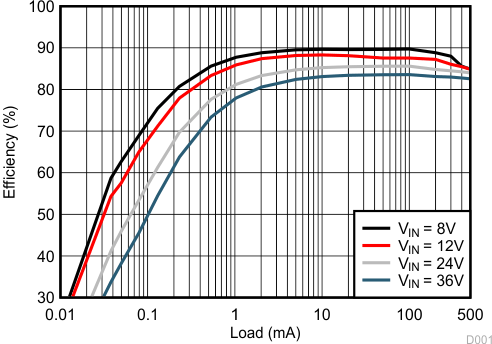
| LF = 22 µH COUT = 200 µF |
FSW(nom) = 100 kHz RRT = 0 Ω |
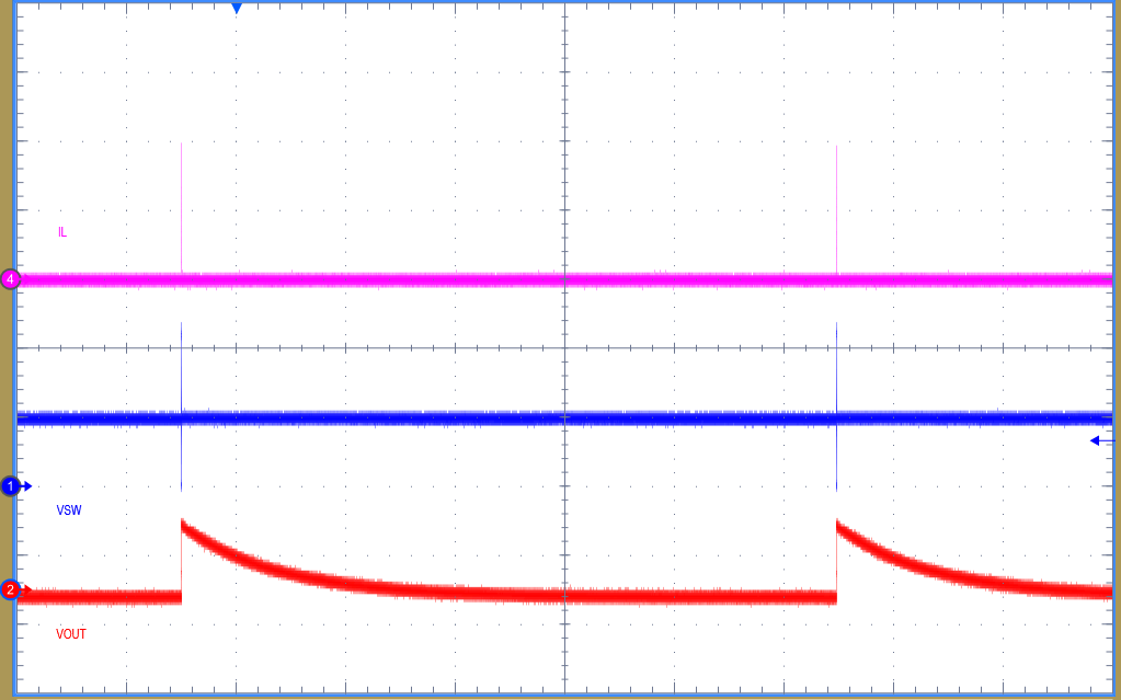
| Time Scale: 50 ms/Div CH1: VSW, 5 V/Div |
CH2: VOUT, 50 mV/Div CH4: IL, 0.4 A/Div |
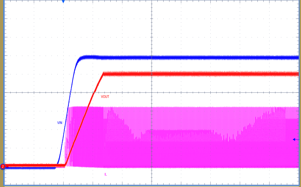
| Time Scale: 2 ms/Div CH1: VIN, 2 V/Div |
CH2: VOUT, 1 V/Div CH4: IL, 0.4 A/Div |
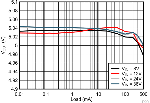
| LF = 22 µH COUT = 200 µF |
FSW(nom) = 100 kHz RRT = 0 Ω |
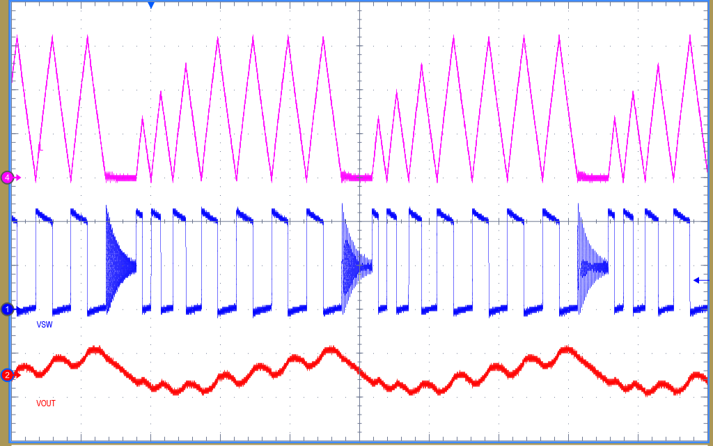
| Time Scale: 20 µs/Div CH1: VSW, 5 V/Div |
CH2: VOUT, 100 mV/Div CH4: IL, 0.4 A/Div |
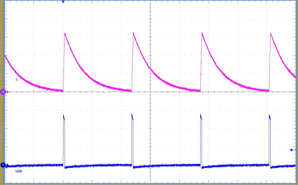
| Time Scale: 50 µs/Div CH1: VSW, 4 V/Div |
CH4: IL, 0.4 A/Div |
8.2.5 Design 5: 12-V, 300-mA COT Converter Operating From 24-V or 48-V Input
The schematic diagram of 12-V, 300-mA COT converter is given in Figure 84.
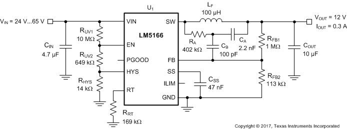 Figure 84. Schematic for Design 5 With VOUT = 12 V, IOUT(max) = 300 mA, FSW(nom) = 400 kHz
8.2.5.1 Design Requirements
The full-load efficiency specifications are 93% and 89% based on input voltages of 24 V and 48 V, respectively, and an output voltage setpoint of 12 V. The input voltage range is 24 V to 65 V, with UVLO turnon and turnoff at 20 V and 18 V, respectively. The output voltage setpoint is established by feedback resistors, RFB1 and RFB2. The required components are listed in Table 8.
Table 8. List of Components for Design 5(1)
| REF DES | QTY | SPECIFICATION | VENDOR | PART NUMBER |
|---|---|---|---|---|
| CIN | 1 | 4.7 µF, 100 V, X7S, 1210 | Murata | GRM31CR71H475MA12L |
| 4.7 µF, 80 V, X7R, 1210 | Murata | GRM32ER71K475KE14L | ||
| COUT | 1 | 10 µF, 25 V, X7R, 1206 | Murata | GRM31CR71E106MA12L |
| TDK | C3216X7R1E106M | |||
| Würth | 885012208069 | |||
| LF | 1 | 100 µH ±20%, 0.54 A, 375 mΩ maximum DCR, 6 × 6 × 3.5 mm | Coilcraft | LPS6235-104MRC |
| RA | 1 | 402 kΩ, 1%, 0402 | Std | Std |
| RFB1 | 1 | 1 MΩ, 1%, 0402 | Std | Std |
| RFB2 | 1 | 113 kΩ, 1%, 0402 | Std | Std |
| RUV1 | 1 | 10 MΩ, 1%, 0603 | Std | Std |
| RUV2 | 1 | 649 kΩ, 1%, 0402 | Std | Std |
| RHYS | 1 | 14 kΩ, 1%, 0402 | Std | Std |
| RRT | 1 | 169 kΩ, 1%, 0402 | Std | Std |
| CA | 1 | 2.2 nF, 25 V, X7R, 0402 | Std | Std |
| CB | 1 | 100 pF, 50 V, NP0, 0402 | Std | Std |
| CSS | 1 | 47 nF, 16 V, X7R, 0402 | Std | Std |
| U1 | 1 | LM5166 Synchronous Buck Converter, VSON-10, 3 mm × 3 mm | TI | LM5166DRCR |
8.2.5.2 Detailed Design Procedure
The component selection procedure for this design is quite similar to that of COT designs 1 and 2.
8.2.5.2.1 Peak Current Limit Setting – RILIM
Leave the ILIM pin open circuit to select the 500-mA peak current limit setting for a rated output current of 300 mA. See Table 3.
8.2.5.2.2 Switching Frequency – RRT
Using Equation 4, select a standard 1% resistor value of 169 kΩ to set a switching frequency of 400 kHz.
8.2.5.2.3 Inductor – LF
Choosing a 100-μH inductor in this design results in 150-mA peak-to-peak ripple current at an input voltage of 24 V, equivalent to 50% of the 300-mA rated load current. A larger ripple current design results in improved light-load efficiency. The peak inductor current at maximum input voltage of 65 V is 424 mA, which is sufficiently below the LM5166 peak current limit of 500 mA. Select an inductor with saturation current rating well above the peak current limit setting, and allow for derating of the saturation current at the highest expected operating temperature.
8.2.5.2.4 Input and Output Capacitors – CIN, COUT
Choose a 4.7-µF, 80-V or 100-V ceramic input capacitor with 1210 footprint. Such a capacitor is typically available in X7S or X7R dielectric. Based on Equation 24, select a 10-µF, 25-V ceramic output capacitor with X7R dielectric and 1206 footprint.
8.2.5.2.5 Feedback Resistors – RFB1, RFB2
Select RFB1 of 1 MΩ to minimize quiescent current and improve light-load efficiency in this application. With the desired output voltage setpoint of 12 V and VFB = 1.223 V, calculate the resistance of RFB2 using Equation 15 as 113.5 kΩ. Choose the closest available standard value of 113 kΩ for RFB2. See Adjustable Output Voltage (FB) for more detail.
8.2.5.2.6 Ripple Generation Network – RA, CA, CB
Select the ripple injection circuit components RA and CA values using Equation 10 and Equation 11. Choose capacitor CB using Equation 12 based on a target transient response settling time of 300 µs.
8.2.5.2.7 Undervoltage Lockout Setpoint – RUV1, RUV2, RHYS
Adjust the undervoltage lockout (UVLO) using an externally-connected resistor divider network of RUV1, RUV2, and RHYS. The UVLO has two thresholds, one for power up when the input voltage is rising and one for power down or brownouts when the input voltage is falling. The EN rising threshold for the LM5166 is 1.22 V.
Rearranging Equation 16 and Equation 17, the expressions to calculate RUV2 and RHYS are as follows:


Choose RUV1 as 10 MΩ to minimize input quiescent current. Given the desired input voltage UVLO thresholds of 20 V and 18 V, calculate the resistance of RUV2 and RHYS as 649 kΩ and 14 kΩ, respectively. See Precision Enable (EN) and Hysteresis (HYS) for more detail.
8.2.5.2.8 Soft Start – CSS
Install a 47-nF capacitor from SS to GND for a soft-start time of 6 ms.
8.2.5.3 Application Curves
Unless otherwise stated, application curves were taken at TA = 25°C.
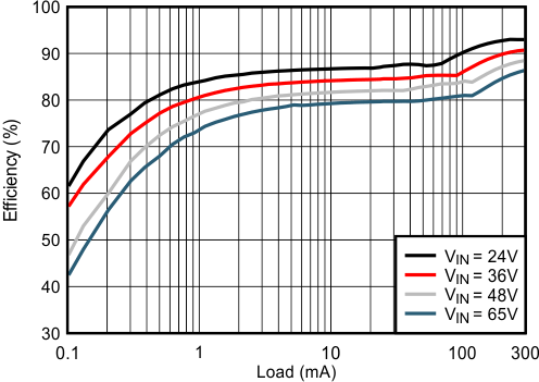 Figure 85. Converter Efficiency
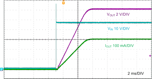
| Time Scale: 2 ms/Div CH2: VIN, 10 V/Div |
CH3: VOUT, 2 V/Div CH4: IOUT, 0.1 A/Div |
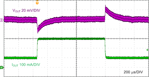
| Time Scale: 200 µs/Div CH3: VOUT, 20 mV/Div |
CH4: IOUT, 0.1 A/Div |
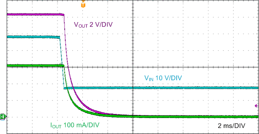
| Time Scale: 2 ms/Div CH2: VIN, 10 V/Div |
CH3: VOUT, 2 V/Div CH4: IL, 0.1 A/Div |