SNVSAR0 November 2016 LM53602 , LM53603
PRODUCTION DATA.
- 1 Features
- 2 Applications
- 3 Description
- 4 Revision History
- 5 Device Comparison Table
- 6 Pin Configuration and Functions
- 7 Specifications
- 8 Detailed Description
- 9 Application and Implementation
- 10Power Supply Recommendations
- 11Layout
- 12Device and Documentation Support
- 13Mechanical, Packaging, and Orderable Information
Package Options
Mechanical Data (Package|Pins)
- PWP|16
Thermal pad, mechanical data (Package|Pins)
- PWP|16
Orderable Information
9 Application and Implementation
NOTE
Information in the following applications sections is not part of the TI component specification, and TI does not warrant its accuracy or completeness. TI's customers are responsible for determining the suitability of components for their purposes. Customers should validate and test their design implementation to confirm system functionality.
9.1 Application Information
The LM53603 and LM53602 are step-down DC-DC converters, typically used to convert a higher DC voltage to a lower DC voltage with a maximum output current of either 3 A or 2 A. The following design procedure can be used to select components for the LM53603 or LM53602. Alternately, the WEBENCH® Design Tool may be used to generate a complete design. This tool uses an iterative design procedure and has access to a comprehensive database of components. This allows the tool to create an optimized design and allows the user to experiment with various design options.
9.2 Typical Applications
9.2.1 Typical and Full-Featured Industrial Application Circuits
Figure 15 shows the minimum required application circuit for the fixed output voltage versions, while Figure 16 shows the connections for complete processor control of the LM53603. See these figures while following the design procedures. Table 2 provides an example of typical design requirements.
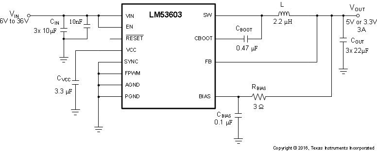 Figure 15. Typical Industrial Power Supply Schematic
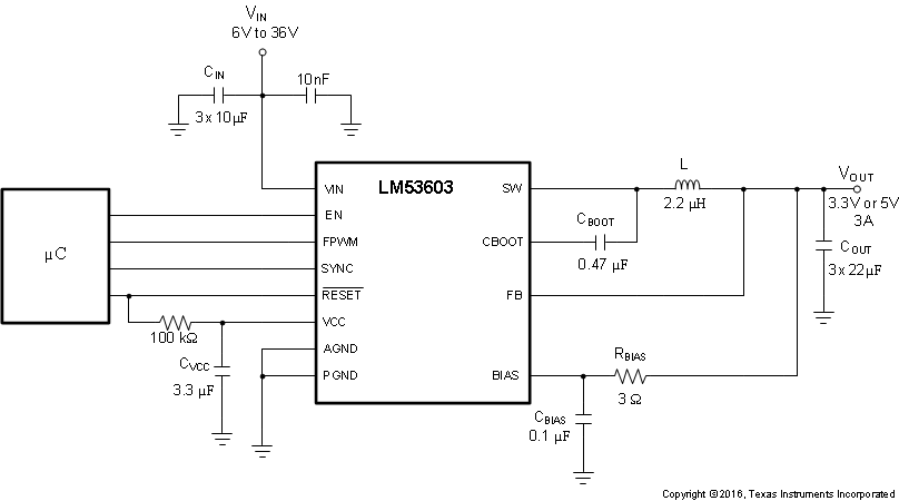 Figure 16. Full-Featured Industrial Power Supply Schematic
9.2.1.1 Design Parameters
There are a few design parameters to take into account. Most of those choices decide which version of the device to use. The desired output current steers the designer toward a LM53602 type or LM53603 type part. If the output voltage is 3.3 V or 5 V, a fixed output version of the device can be used. Any other voltage level within the tolerance of the part can be achieved by using an adjustable version of the device. Most but not all parameters are independent of the of the IC choice. The output filter components (inductor and output capacitors) might vary with the choice of output voltage, especially for output voltages higher than 5 V. See Detailed Design Procedure for help in choosing these components.
Table 2. Design Parameters
| DESIGN PARAMETER | EXAMPLE VALUE |
|---|---|
| Input voltage | 12 V |
| Output voltage | 5 V |
| Maximum output current | 3 A |
9.2.1.2 Detailed Design Procedure
The following detailed design procedure applies to Figure 15, Figure 16, and Figure 45.
9.2.1.2.1 Setting the Output Voltage
For the fixed output voltage versions, the FB input is connected directly to the output voltage node. Preferably, near the top of the output capacitor. If the feed-back point is located further away from the output capacitors (that is, remote sensing), then a small 100-nF capacitor may be needed at the sensing point.
For output voltages other than 5 V or 3.3 V, a feedback divider is required. For the ADJ version of the device, the regulator holds the FB pin at 1 V. The range of adjustable output voltage can be found in the Recommended Operating Conditions. Equation 3 can be used to determine RFBB for a desired output voltage and a given RFBT. Usually RFBT is limited to a maximum value of 100 kΩ.

In addition, a feed-forward capacitor CFF may be required to optimize the transient response. For output voltages greater than 6 V, the WEBENCH Design Tool can be used to optimize the design. Recommended CFF values for some cases are given in the table below. It is important to note that these values provide a first approximation only and need to be verified for each application by the designer.
Table 3. Recommended CFFcapacitors
| VOUT | COUT (nominal)(1) | L | RFBT | RFBB | CFF |
|---|---|---|---|---|---|
| 3.2V | 44µF | 2.2µH | 69.8kΩ | 31.6kΩ | 33pF |
| 3.2V | 110µF | 2.2µH | 69.8kΩ | 31.6kΩ | 120pF |
| 5.1V | 44µF | 2.2µH | 80.6kΩ | 19.6kΩ | 33pF |
| 5.1V | 110µF | 2.2µH | 80.6kΩ | 19.6kΩ | 220pF |
| 8V | 66µF | 4.7µH | 86.6kΩ | 12.4kΩ | 120pF |
| 8V | 100µF | 4.7µH | 86.6kΩ | 12.4kΩ | 220pF |
| 10V | 66µF | 4.7µH | 90.9kΩ | 10.0kΩ | 120pF |
9.2.1.2.2 Output Capacitors
The LM53603 is designed to work with low-ESR ceramic capacitors. The effective value of these capacitors is defined as the actual capacitance under voltage bias and temperature. All ceramic capacitors have a large voltage coefficient, in addition to normal tolerances and temperature coefficients. Under DC bias, the capacitance value drops considerably. Larger case sizes or higher voltage capacitors are better in this regard. To help mitigate these effects, multiple small capacitors can be used in parallel to bring the minimum effective capacitance up to the desired value. This can also ease the RMS current requirements on a single capacitor. Table 4 shows the nominal and minimum values of total output capacitance recommended for the LM53603. The values shown also provide a starting point for other output voltages, when using the ADJ option. Also shown are the measured values of effective capacitance for the indicated capacitor. More output capacitance can be used to improve transient performance and reduce output voltage ripple.
In practice, the output capacitor has the most influence on the transient response and loop phase margin. Load transient testing and Bode plots are the best way to validate any given design, and should always be completed before the application goes into production. A careful study of temperature and bias voltage variation of any candidate ceramic capacitor should be made to ensure that the minimum value of effective capacitance is provided. The best way to obtain an optimum design is to use the Texas Instruments WEBENCH Design Tool.
In ADJ applications the feed-forward capacitor, CFF, provides another degree of freedom when stabilizing and optimizing the design. Application report Optimizing Transient Response of Internally Compensated dc-dc Converters With Feedforward Capacitor (SLVA289) should prove helpful when adjusting the feed-forward capacitor.
In addition to the capacitance shown in Table 4, a small ceramic capacitor placed on the output can help to reduce high frequency noise. Small case size ceramic capacitors in the range of 1 nF to 100 nF can be very helpful in reducing spikes on the output caused by inductor parasitics.
The maximum value of total output capacitance should be limited to between 300 µF and 400 µF. Large values of output capacitance can prevent the regulator from starting-up correctly and adversely effect the loop stability. If values in the range given above, or greater, are to be used, then a careful study of start-up at full load and loop stability must be performed.
Table 4. Recommended Output Capacitors
| OUTPUT VOLTAGE | NOMINAL OUTPUT CAPACITANCE | MINIMUM OUTPUT CAPACITANCE | PART NUMBER (MANUFACTURER) | ||
|---|---|---|---|---|---|
| RATED CAPACITANCE | MEASURED CAPACITANCE(1) | RATED CAPACITANCE | MEASURED CAPACITANCE(1) | ||
| 3.3 V | 3 × 22 µF | 63 µF | 2 × 22 µF | 42 µF | C3225X7R1C226M250AC (TDK) |
| 5 V | 3 × 22 µF | 60 µF | 2 × 22 µF | 40 µF | C3225X7R1C226M250AC (TDK) |
| 6 V | 3 × 22 µF | 59 µF | 2 × 22 µF | 39 µF | C3225X7R1C226M250AC (TDK) |
| 10 V(2) | 3 × 22 µF | 48 µF | 2 × 22 µF | 32 µF | C3225X7R1C226M250AC (TDK) |
9.2.1.2.3 Input Capacitors
The ceramic input capacitors provide a low impedance source to the regulator in addition to supplying ripple current and isolating switching noise from other circuits. Table 5 shows the nominal and minimum values of total input capacitance recommenced for the LM53603. Also shown are the measured values of effective capacitance for the indicated capacitor. In addition, small high frequency bypass capacitors connected directly between the VIN and PGND pins are very helpful in reducing noise spikes and aid in reducing conducted EMI. TI recommends that a small case size 10-nF ceramic capacitor be placed across the input, as close as possible to the device (see Figure 47). Additional high frequency capacitors can be used to help manage conducted EMI or voltage spike issues that may be encountered.
Table 5. Recommended Input Capacitors
| NOMINAL INPUT CAPACITANCE | MINIMUM INPUT CAPACITANCE | PART NUMBER (MANUFACTURER) | ||
|---|---|---|---|---|
| RATED CAPACITANCE | MEASURED CAPACITANCE (1) | RATED CAPACITANCE | MEASURED CAPACITANCE(1) | |
| 3 x 10 µF | 22.5 µF | 2 × 10 µF | 15 µF | CL32B106KBJNNNE (Samsung) |
Many times it is desirable to use an electrolytic capacitor on the input, in parallel with the ceramics. This is especially true if longs leads or traces are used to connect the input supply to the regulator. The moderate ESR of this capacitor can help damp any ringing on the input supply caused by long power leads. The use of this additional capacitor also helps with voltage dips caused by input supplies with unusually high impedance.
Most of the input switching current passes through the ceramic input capacitor(s). The approximate RMS value of this current can be calculated from Equation 4 and should be checked against the manufacturers' maximum ratings.

9.2.1.2.4 Inductor
The LM53603 and LM53602 are optimized for a nominal inductance of 2.2 µH for the 5-V and 3.3-V versions. This gives a ripple current that is approximately 20% to 30% of the full load current of 3 A. For output voltages greater than 5 V, a proportionally larger inductor can be used. This keeps the ratio of inductor current slope to internal compensating slope constant.
The most important inductor parameters are saturation current and parasitic resistance. Inductors with a saturation current of between 5 A and 6 A are appropriate for most applications, when using the LM53603. For the LM53602, inductors with a saturation current of between 4 A and 5 A are appropriate. Of course the inductor parasitic resistance should be as low as possible to reduce losses at heavy loads. Table 6 gives a list of several possible inductors that can be used with the LM53603.
Table 6. Recommenced Inductors
| MANUFACTURER | PART NUMBER | SATURATION CURRENT | DC RESISTANCE |
|---|---|---|---|
| Würth | 7440650022 | 6 A | 15 mΩ |
| Coilcraft | DO3316T-222MLB | 7.8 A | 11 mΩ |
| Coiltronics | MPI4040R3-2R2-R | 7.9 A | 48 mΩ |
| Vishay | IHLP2525CZER2R2M01 | 14 A | 18 mΩ |
| Vishay | IHLP2525BDER2R2M01 | 14 A | 28 mΩ |
| Coilcraft | XAL6030-222ME | 16 A | 13 mΩ |
9.2.1.2.5 VCC
The VCC pin is the output of the internal LDO, used to supply the control circuits of the LM53603. This output requires a 3.3-µF to 4.7-µF, ceramic capacitor connected from VCC to GND for proper operation. An X7R device with a rating of 10 V is highly recommended. In general this output should not be loaded with any external circuitry. However, it can be used to supply a logic level to the FPWM input, or for the pullup resistor used with the RESET output (see Figure 16). The nominal output of the LDO is 3.15 V.
9.2.1.2.6 BIAS
The BIAS pin is the input to the internal LDO. As mentioned in Input Supply Current, this input is connected to VOUT to provide the lowest possible supply current at light loads. Because this input is connected directly to the output, it should be protected from negative voltage transients. Such transients may occur when the output is shorted at the end of a long PCB trace or cable. If this is likely, in a given application, then a small resistor should be placed in series between the BIAS input and VOUT, as shown in Figure 15. The resistor should be sized to limit the current out of the BIAS pin to <100 mA. Values in the range of 2 Ω to 5 Ω are usually sufficient. Values greater than 5 Ω are not recommended. As a rough estimate, assume that the full negative transient appears across RBIAS and design for a current of < 100 mA. In severe cases, a Schottky diode can be placed in parallel with the output to limit the transient voltage and current.
9.2.1.2.7 CBOOT
The LM53603 requires a boot-strap capacitor between the CBOOT pin and the SW pin. This capacitor stores energy that is used to supply the gate drivers for the power MOSFETs. A ceramic capacitor of 0.47 µF, ≥ 6.3 V is required. A 10-V rated capacitor or higher is highly recommended.
9.2.1.2.8 Maximum Ambient Temperature
As with any power conversion device, the LM53603 dissipates internal power while operating. The effect of this power dissipation is to raise the internal temperature of the converter, above ambient. The internal die temperature (TJ) is a function of the ambient temperature, the power loss and the effective thermal resistance, RθJA of the device and PCB combination. The maximum internal die temperature for the LM53603 is 150°C, thus establishing a limit on the maximum device power dissipation and therefore load current at high ambient temperatures. Equation 5 shows the relationships between the important parameters.

It is easy to see that larger ambient temperatures (TA) and larger values of RθJA reduce the maximum available output current. As stated in Semiconductor and IC Package Thermal Metrics, the values given in the Thermal Information table are not valid for design purposes and must not be used to estimate the thermal performance of the application. The values reported in that table were measured under a specific set of conditions that are never obtained in an actual application. The effective RθJA is a critical parameter and depends on many factors such as power dissipation, air temperature, PCB area, copper heat sink area, number of thermal vias under the package, air flow, and adjacent component placement. The LM53603 uses an advanced package with a heat spreading pad (EP) on the bottom. This must be soldered directly to the PCB copper ground plane to provide an effective heat sink, as well as a proper electrical connection. The resources in Ground and Thermal Plane Considerations can be used as a guide to optimal thermal PCB design and estimating RθJA for a given application environment. A typical example of RθJA versus copper board area is shown in Figure 17. The copper area in this graph is that for each layer of a four-layer board; the inner layers are 1 oz. (35 µm), while the outer layers are 2 oz. (70 µm). A typical curve of maximum load current versus ambient temperature, for both the LM53603 and LM53602, is shown in Figure 18. This data was taken with the device soldered to a PCB with an RθJA of about 17°C/W and an input voltage of 12 V. It must be remembered that the data shown in these graphs are for illustration only and the actual performance in any given application depends on all of the factors mentioned above.
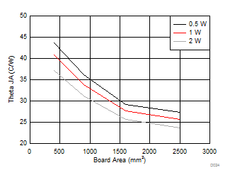
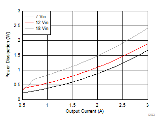 Figure 19. IC Power Dissipation vs Output Current for 3.3-V output
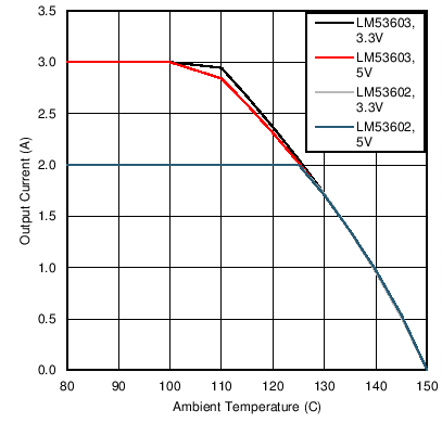 Figure 18. Maximum Output Current vs Ambient Temperature
 RθJA = 17°C/W, VIN = 12 V
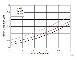 Figure 20. IC Power Dissipation vs Output Current for 5-V output
9.2.1.3 Application Curves
The following characteristics apply only to the circuit of Figure 15. These parameters are not tested and represent typical performance only. Unless otherwise stated, the following conditions apply: VIN = 12 V, TA = 25°C.
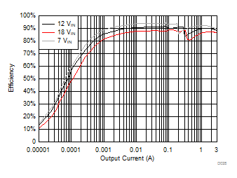
| VOUT = 5 V | AUTO | |
| Inductor = XAL6030-222ME | ||
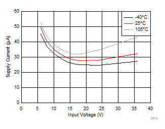
| VOUT = 5 V | AUTO | IOUT = 0 A |
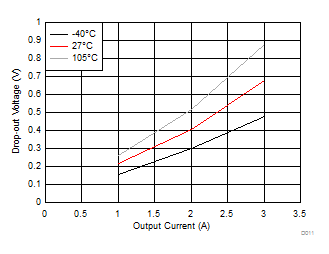
| VOUT = 5 V |
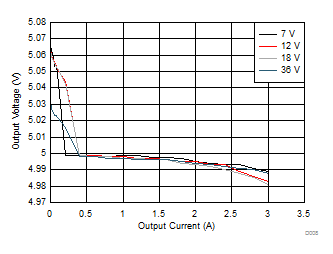
| VOUT = 5 V | AUTO | |
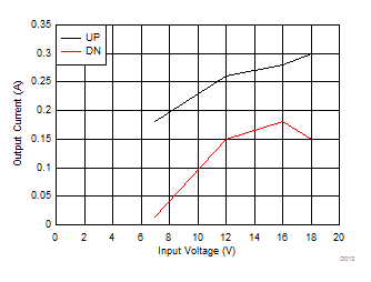
| VOUT = 5 V |
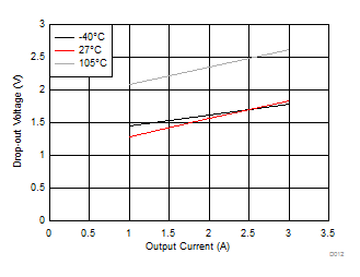
| VOUT = 5 V |
The following characteristics apply only to the circuit of Figure 15. These parameters are not tested and represent typical performance only. Unless otherwise stated, the following conditions apply: VIN = 12 V, TA = 25°C.
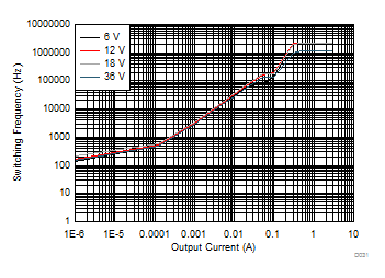
| VOUT = 5 V | AUTO |
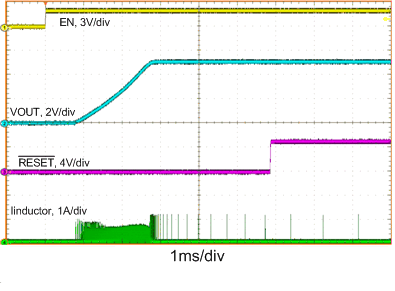
| VOUT = 5 V | IOUT = 0 A | AUTO |
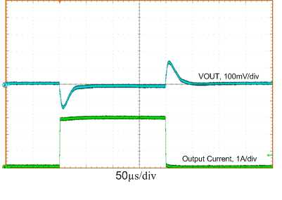
| VOUT = 5 V | IOUT = 0 A to 3 A, TR = TF = 1 µs | FPWM |
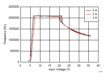
| VOUT = 5 V | FPWM |
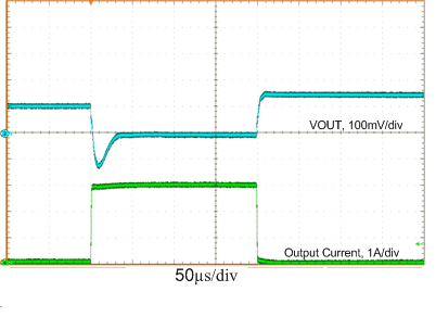
| VOUT = 5 V | IOUT = 0 A to 3 A, TR = TF = 1 µs | AUTO |
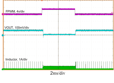
| VOUT = 5 V | IOUT = 1 mA |
The following characteristics apply only to the circuit of Figure 15. These parameters are not tested and represent typical performance only. Unless otherwise stated, the following conditions apply: VIN = 12 V, TA = 25°C.
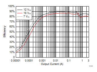
| VOUT = 3.3 V | AUTO | |
| Inductor = XAL6030-222ME | ||
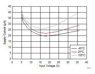
| VOUT = 3.3 V | AUTO | IOUT = 0 A |
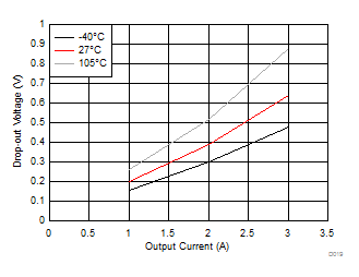
| VOUT = 3.3 V |
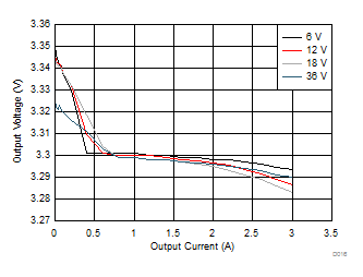
| VOUT = 3.3 V | AUTO | |
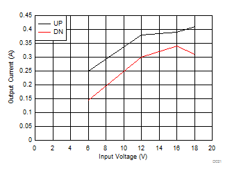
| VOUT = 3.3 V |
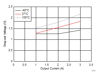
| VOUT = 3.3 V |
The following characteristics apply only to the circuit of Figure 15. These parameters are not tested and represent typical performance only. Unless otherwise stated, the following conditions apply: VIN = 12 V, TA = 25°C.
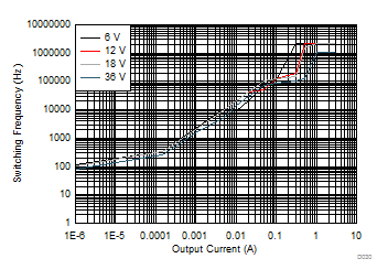
| VOUT = 3.3 V | AUTO |
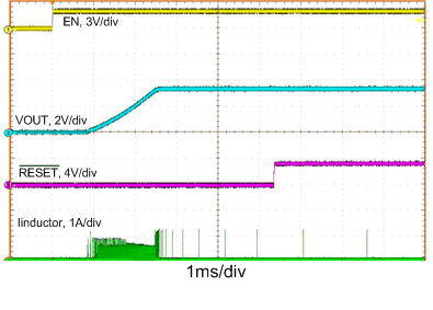
| VOUT = 3.3 V | AUTO | IOUT = 0 A |
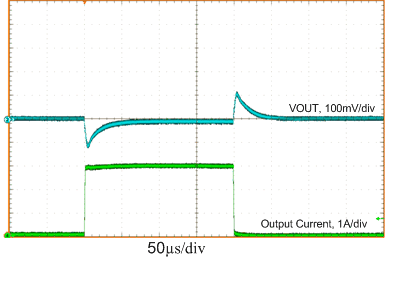
| VOUT = 3.3 V | IOUT = 0 A to 3 A, TR = TF = 1 µs | FPWM |
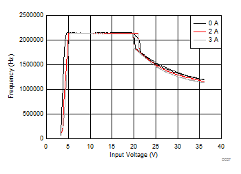
| VOUT = 3.3 V | FPWM |
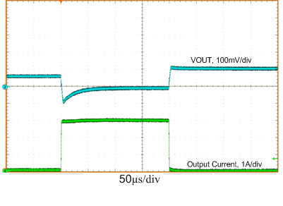
| VOUT = 3.3 V | IOUT = 0 A to 3 A, TR = TF = 1 µs | AUTO |
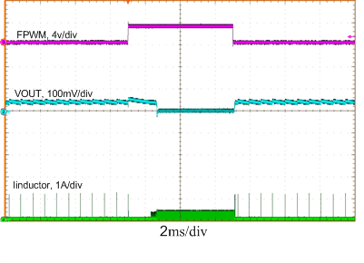
| VOUT = 3.3 V | IOUT = 1 mA |
9.3 Typical Adjustable Industrial Application Circuit
Figure 45 shows a typical example of a design with an output voltage of 10 V; while Table 7 gives typical design parameters. See Detailed Design Procedure for the design procedure.
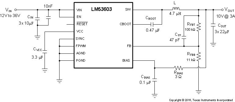 Figure 45. Typical Adjustable Output Industrial Power Supply Schematic
CD/DVD/Blu-ray Disc™ Motor Drive Applications
VOUT = 10 V
9.3.1 Design Parameters for Typical Adjustable Output Industrial Power Supply
There are a few design parameters to take into account. Most of those choices decide which version of the device to use. The desired output current steers the designer toward a LM53602 type or LM53603 type part. Most but not all parameters are independent of the of the IC choice. The output filter components (inductor and output capacitors) might vary with the choice of output voltage, especially for output voltages higher than 5 V. Refer to Detailed Design Procedure for details on choosing the components for the application.
Table 7. Design Parameters
| DESIGN PARAMETER | EXAMPLE VALUE |
|---|---|
| Input Voltage | 12 V |
| Output Voltage | 10 V |
| Maximum Output Current | 3 A |
9.4 Do's and Don't's
- Don't: Exceed the Absolute Maximum Ratings.
- Don't: Exceed the ESD Ratings.
- Don't: Exceed the Recommended Operating Conditions.
- Don't: Allow the EN, FPWM or SYNC input to float.
- Don't: Allow the output voltage to exceed the input voltage, nor go below ground.
- Don't: Use the thermal data given in the Thermal Information table to design your application.
- Do: Follow all of the guidelines and suggestions found in this data sheet, before committing your design to production. TI Application Engineers are ready to help critique your design and PCB layout to help make your project a success.
- Do: Refer to the helpful documents found in Layout Guidelines and Ground and Thermal Plane Considerations.