SNIS152E May 2009 – July 2015 LM57
PRODUCTION DATA.
- 1 Features
- 2 Applications
- 3 Description
- 4 Revision History
- 5 Device Comparison Table
- 6 Pin Configuration and Functions
-
7 Specifications
- 7.1 Absolute Maximum Ratings
- 7.2 ESD Ratings
- 7.3 Recommended Operating Conditions
- 7.4 Thermal Information
- 7.5 Electrical Characteristics - Accuracy Characteristics - Trip Point Accuracy
- 7.6 Electrical Characteristics - Accuracy Characteristics - VTEMP Analog Temperature Sensor Output Accuracy
- 7.7 Electrical Characteristics
- 7.8 Switching Characteristics
- 7.9 Typical Characteristics
-
8 Detailed Description
- 8.1 Overview
- 8.2 Functional Block Diagram
- 8.3 Feature Description
- 8.4 Device Functional Modes
- 9 Application and Implementation
- 10Power Supply Recommendations
- 11Layout
- 12Device and Documentation Support
- 13Mechanical, Packaging, and Orderable Information
Package Options
Mechanical Data (Package|Pins)
Thermal pad, mechanical data (Package|Pins)
Orderable Information
8 Detailed Description
8.1 Overview
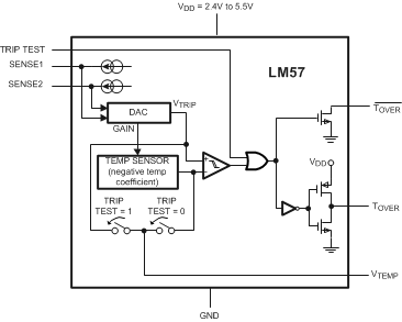
The LM57 is a precision, dual-output, temperature switch with analog temperature sensor output. The trip temperature (TTRIP) is selected from 256 possible values by using two external 1% resistors. The VTEMP class AB analog output provides a voltage that is proportional to temperature. The LM57 includes an internal reference DAC, analog temperature sensor and analog comparator. The reference DAC is connected to one of the comparator inputs. The reference DAC output voltage (VTRIP) is controlled by the value of resistance applied to the SENSE pins. The resistance value sets one of 16 "logic" levels at the SENSE pins. These "logic" levels are then decoded and applied to the DAC input, thus the actual resistance tolerance does not directly affect the threshold level accuracy. The result of the reference DAC voltage and the temperature sensor output comparison is provided on two output pins TOVER and TOVER.
The VTEMP output has a programmable gain. The output gain has 4 possible settings as described in Figure 12. The gain setting is dependent on the trip point selected by resistance applied to the SENSE pins.
Built-in temperature hysteresis (THYST) prevents the digital outputs from oscillating. The TOVER and TOVER will activate when the die temperature exceeds TTRIP and will release when the temperature falls below a temperature equal to TTRIP minus THYST. TOVER is active-high with a push-pull structure. TOVER, is active-low with an open-drain structure. There are two different hysteresis options available that are factory preset. The preset hysteresis can be selected by purchasing the proper order number as described in Device Comparison Table.
Driving the TRIP-TEST high will activate the digital outputs. A processor can check the logic level of the TOVER or TOVER, confirming that they changed to their active state. This allows for system production testing verification that the comparator and output circuitry are functional after system assembly. When the TRIP-TEST pin is high, the trip-level reference voltage appears at the VTEMP pin. Tying TOVER to TRIP-TEST will latch the output after it trips. It can be cleared by forcing TRIP-TEST low or powering off the LM57.
8.2 Functional Block Diagram
8.3 Feature Description
8.3.1 LM57 VTEMP Temperature-to-Voltage Transfer Function
The value of the RSENSE resistors select a trip point and a corresponding VTEMP gain (J2, J3, J4, or J5).The trip point range associated with a given gain is shown in bold green in Table 1. The VTEMP gain is selected by the RSENSE resistors. VTEMP is valid over the entire temperature range. The VTEMP gain is selected by the RSENSE resistors. VTEMP is valid over the entire temperature range.
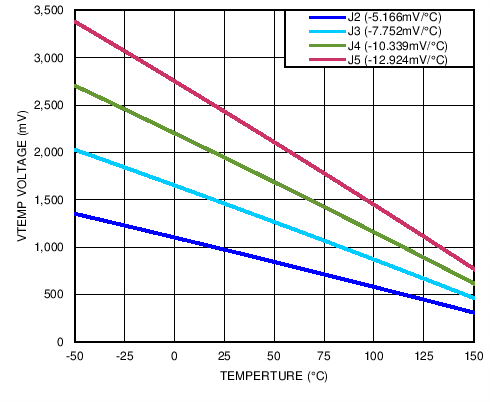 Figure 12. Temperature Transfer Characteristics
Table 1. LM57 VTEMP Temperature to Voltage (1)
| Temperature (°C) | VTEMP VOLTAGE (mV) | |||
|---|---|---|---|---|
| J2 (-5.166 mV/°C) | J3 (–7.752 mV/°C) | J4 (–10.339 mV/°C) | J5 (–12.924 mV/°C) | |
| –50 | 1352.56 | 2028.80 | 2705.20 | 3381.40 |
| –49 | 1347.60 | 2021.35 | 2695.26 | 3368.98 |
| –48 | 1342.64 | 2013.90 | 2685.32 | 3356.55 |
| –47 | 1337.67 | 2006.44 | 2675.38 | 3344.12 |
| –46 | 1332.70 | 1998.98 | 2665.43 | 3331.68 |
| –45 | 1327.73 | 1991.52 | 2655.47 | 3319.23 |
| –44 | 1322.76 | 1984.05 | 2645.51 | 3306.78 |
| –43 | 1317.78 | 1976.58 | 2635.54 | 3294.32 |
| –42 | 1312.81 | 1969.11 | 2625.57 | 3281.85 |
| –41 | 1307.82 | 1961.63 | 2615.60 | 3269.38 |
| –40 | 1302.84 | 1954.15 | 2605.62 | 3256.90 |
| –39 | 1297.86 | 1946.66 | 2595.63 | 3244.41 |
| –38 | 1292.87 | 1939.17 | 2585.64 | 3231.92 |
| –37 | 1287.88 | 1931.68 | 2575.64 | 3219.42 |
| –36 | 1282.88 | 1924.18 | 2565.64 | 3206.92 |
| –35 | 1277.89 | 1916.68 | 2555.63 | 3194.41 |
| –34 | 1272.89 | 1909.17 | 2545.62 | 3181.89 |
| –33 | 1267.88 | 1901.66 | 2535.60 | 3169.37 |
| –32 | 1262.88 | 1894.15 | 2525.58 | 3156.84 |
| –31 | 1257.87 | 1886.63 | 2515.56 | 3144.30 |
| –30 | 1252.86 | 1879.11 | 2505.52 | 3131.76 |
| –29 | 1247.85 | 1871.59 | 2495.49 | 3119.21 |
| –28 | 1242.84 | 1864.06 | 2485.44 | 3106.66 |
| –27 | 1237.82 | 1856.53 | 2475.40 | 3094.10 |
| –26 | 1232.80 | 1848.99 | 2465.34 | 3081.53 |
| –25 | 1227.78 | 1841.45 | 2455.29 | 3068.96 |
| –24 | 1222.75 | 1833.91 | 2445.23 | 3056.38 |
| –23 | 1217.73 | 1826.36 | 2435.16 | 3043.79 |
| –22 | 1212.70 | 1818.81 | 2425.09 | 3031.20 |
| –21 | 1207.67 | 1811.26 | 2415.01 | 3018.60 |
| –20 | 1202.63 | 1803.70 | 2404.93 | 3006.00 |
| –19 | 1197.59 | 1796.13 | 2394.84 | 2993.38 |
| –18 | 1192.55 | 1788.57 | 2384.74 | 2980.77 |
| –17 | 1187.51 | 1781.00 | 2374.65 | 2968.14 |
| –16 | 1182.46 | 1773.42 | 2364.54 | 2955.51 |
| –15 | 1177.42 | 1765.85 | 2354.44 | 2942.87 |
| –14 | 1172.37 | 1758.26 | 2344.32 | 2930.23 |
| –13 | 1167.31 | 1750.68 | 2334.20 | 2917.58 |
| –12 | 1162.26 | 1743.09 | 2324.08 | 2904.93 |
| –11 | 1157.20 | 1735.50 | 2313.95 | 2892.26 |
| –10 | 1152.14 | 1727.90 | 2303.82 | 2879.60 |
| –9 | 1147.07 | 1720.30 | 2293.68 | 2866.92 |
| –8 | 1142.01 | 1712.69 | 2283.54 | 2854.24 |
| –7 | 1136.94 | 1705.09 | 2273.39 | 2841.55 |
| –6 | 1131.87 | 1697.47 | 2263.24 | 2828.86 |
| –5 | 1126.79 | 1689.86 | 2253.08 | 2816.16 |
| –4 | 1121.72 | 1682.24 | 2242.91 | 2803.45 |
| –3 | 1116.64 | 1674.61 | 2232.74 | 2790.74 |
| –2 | 1111.56 | 1666.99 | 2222.57 | 2778.02 |
| –1 | 1106.47 | 1659.35 | 2212.39 | 2765.30 |
| 0 | 1101.39 | 1651.72 | 2202.21 | 2752.57 |
| 1 | 1096.30 | 1644.08 | 2192.02 | 2739.83 |
| 2 | 1091.20 | 1636.44 | 2181.82 | 2727.08 |
| 3 | 1086.11 | 1628.79 | 2171.62 | 2714.33 |
| 4 | 1081.01 | 1621.14 | 2161.42 | 2701.58 |
| 5 | 1075.91 | 1613.48 | 2151.21 | 2688.82 |
| 6 | 1070.81 | 1605.83 | 2141.00 | 2676.05 |
| 7 | 1065.71 | 1598.16 | 2130.78 | 2663.27 |
| 8 | 1060.60 | 1590.50 | 2120.55 | 2650.49 |
| 9 | 1055.49 | 1582.83 | 2110.32 | 2637.70 |
| 10 | 1050.38 | 1575.15 | 2100.09 | 2624.91 |
| 11 | 1045.26 | 1567.48 | 2089.85 | 2612.10 |
| 12 | 1040.14 | 1559.80 | 2079.60 | 2599.30 |
| 13 | 1035.02 | 1552.11 | 2069.35 | 2586.48 |
| 14 | 1029.90 | 1544.42 | 2059.10 | 2573.66 |
| 15 | 1024.77 | 1536.73 | 2048.84 | 2560.84 |
| 16 | 1019.65 | 1529.03 | 2038.57 | 2548.01 |
| 17 | 1014.51 | 1521.33 | 2028.30 | 2535.17 |
| 18 | 1009.38 | 1513.63 | 2018.03 | 2522.32 |
| 19 | 1004.25 | 1505.92 | 2007.75 | 2509.47 |
| 20 | 999.11 | 1498.21 | 1997.46 | 2496.61 |
| 21 | 993.97 | 1490.49 | 1987.17 | 2483.75 |
| 22 | 988.82 | 1482.77 | 1976.88 | 2470.88 |
| 23 | 983.68 | 1475.05 | 1966.58 | 2458.00 |
| 24 | 978.53 | 1467.32 | 1956.27 | 2445.12 |
| 25 | 973.38 | 1459.59 | 1945.96 | 2432.23 |
| 26 | 968.22 | 1451.86 | 1935.64 | 2419.34 |
| 27 | 963.07 | 1444.12 | 1925.32 | 2406.43 |
| 28 | 957.91 | 1436.38 | 1915.00 | 2393.53 |
| 29 | 952.74 | 1428.63 | 1904.67 | 2380.61 |
| 30 | 947.58 | 1420.88 | 1894.33 | 2367.69 |
| 31 | 942.41 | 1413.13 | 1883.99 | 2354.76 |
| 32 | 937.24 | 1405.37 | 1873.64 | 2341.83 |
| 33 | 932.07 | 1397.61 | 1863.29 | 2328.89 |
| 34 | 926.90 | 1389.84 | 1852.94 | 2315.94 |
| 35 | 921.72 | 1382.07 | 1842.57 | 2302.99 |
| 36 | 916.54 | 1374.30 | 1832.21 | 2290.03 |
| 37 | 911.36 | 1366.52 | 1821.84 | 2277.07 |
| 38 | 906.17 | 1358.74 | 1811.46 | 2264.10 |
| 39 | 900.98 | 1350.96 | 1801.08 | 2251.12 |
| 40 | 895.79 | 1343.17 | 1790.69 | 2238.14 |
| 41 | 890.60 | 1335.38 | 1780.30 | 2225.15 |
| 42 | 885.41 | 1327.58 | 1769.90 | 2212.15 |
| 43 | 880.21 | 1319.78 | 1759.50 | 2199.15 |
| 44 | 875.01 | 1311.98 | 1749.09 | 2186.14 |
| 45 | 869.81 | 1304.17 | 1738.68 | 2173.12 |
| 46 | 864.60 | 1296.36 | 1728.26 | 2160.10 |
| 47 | 859.39 | 1288.54 | 1717.84 | 2147.07 |
| 48 | 854.18 | 1280.72 | 1707.41 | 2134.04 |
| 49 | 848.97 | 1272.90 | 1696.98 | 2121.00 |
| 50 | 843.75 | 1265.07 | 1686.54 | 2107.95 |
| 51 | 838.53 | 1257.24 | 1676.10 | 2094.90 |
| 52 | 833.31 | 1249.41 | 1665.65 | 2081.84 |
| 53 | 828.09 | 1241.57 | 1655.20 | 2068.77 |
| 54 | 822.86 | 1233.73 | 1644.74 | 2055.70 |
| 55 | 817.63 | 1225.88 | 1634.28 | 2042.62 |
| 56 | 812.40 | 1218.03 | 1623.81 | 2029.54 |
| 57 | 807.17 | 1210.18 | 1613.34 | 2016.44 |
| 58 | 801.93 | 1202.32 | 1602.86 | 2003.35 |
| 59 | 796.69 | 1194.46 | 1592.38 | 1990.24 |
| 60 | 791.45 | 1186.60 | 1581.89 | 1977.13 |
| 61 | 786.20 | 1178.73 | 1571.40 | 1964.02 |
| 62 | 780.96 | 1170.86 | 1560.90 | 1950.89 |
| 63 | 775.71 | 1162.98 | 1550.40 | 1937.76 |
| 64 | 770.46 | 1155.10 | 1539.89 | 1924.63 |
| 65 | 765.20 | 1147.22 | 1529.37 | 1911.49 |
| 66 | 759.94 | 1139.33 | 1518.86 | 1898.34 |
| 67 | 754.68 | 1131.44 | 1508.33 | 1885.19 |
| 68 | 749.42 | 1123.54 | 1497.80 | 1872.02 |
| 69 | 744.16 | 1115.64 | 1487.27 | 1858.86 |
| 70 | 738.89 | 1107.74 | 1476.73 | 1845.68 |
| 71 | 733.62 | 1099.83 | 1466.19 | 1832.50 |
| 72 | 728.35 | 1091.92 | 1455.64 | 1819.32 |
| 73 | 723.07 | 1084.01 | 1445.08 | 1806.13 |
| 74 | 717.79 | 1076.09 | 1434.53 | 1792.93 |
| 75 | 712.51 | 1068.17 | 1423.96 | 1779.72 |
| 76 | 707.23 | 1060.24 | 1413.39 | 1766.51 |
| 77 | 701.94 | 1052.31 | 1402.82 | 1753.30 |
| 78 | 696.65 | 1044.38 | 1392.24 | 1740.07 |
| 79 | 691.36 | 1036.44 | 1381.65 | 1726.84 |
| 80 | 686.07 | 1028.50 | 1371.07 | 1713.61 |
| 81 | 680.77 | 1020.55 | 1360.47 | 1700.36 |
| 82 | 675.48 | 1012.60 | 1349.87 | 1687.11 |
| 83 | 670.17 | 1004.65 | 1339.27 | 1673.86 |
| 84 | 664.87 | 996.69 | 1328.66 | 1660.60 |
| 85 | 659.56 | 988.73 | 1318.04 | 1647.33 |
| 86 | 654.25 | 980.77 | 1307.42 | 1634.05 |
| 87 | 648.94 | 972.80 | 1296.80 | 1620.77 |
| 88 | 643.63 | 964.83 | 1286.17 | 1607.49 |
| 89 | 638.31 | 956.85 | 1275.53 | 1594.19 |
| 90 | 632.99 | 948.87 | 1264.89 | 1580.89 |
| 91 | 627.67 | 940.89 | 1254.25 | 1567.59 |
| 92 | 622.35 | 932.90 | 1243.60 | 1554.28 |
| 93 | 617.02 | 924.91 | 1232.94 | 1540.96 |
| 94 | 611.69 | 916.92 | 1222.28 | 1527.63 |
| 95 | 606.36 | 908.92 | 1211.61 | 1514.30 |
| 96 | 601.02 | 900.91 | 1200.94 | 1500.97 |
| 97 | 595.69 | 892.91 | 1190.27 | 1487.62 |
| 98 | 590.34 | 884.90 | 1179.59 | 1474.27 |
| 99 | 585.00 | 876.88 | 1168.90 | 1460.92 |
| 100 | 579.66 | 868.87 | 1158.21 | 1447.55 |
| 101 | 574.31 | 860.84 | 1147.52 | 1434.18 |
| 102 | 568.96 | 852.82 | 1136.81 | 1420.81 |
| 103 | 563.61 | 844.79 | 1126.11 | 1407.43 |
| 104 | 558.25 | 836.76 | 1115.40 | 1394.04 |
| 105 | 552.89 | 828.72 | 1104.68 | 1380.65 |
| 106 | 547.53 | 820.68 | 1093.96 | 1367.24 |
| 107 | 542.17 | 812.63 | 1083.23 | 1353.84 |
| 108 | 536.80 | 804.59 | 1072.50 | 1340.42 |
| 109 | 531.43 | 796.53 | 1061.77 | 1327.01 |
| 110 | 526.06 | 788.48 | 1051.02 | 1313.58 |
| 111 | 520.69 | 780.42 | 1040.28 | 1300.15 |
| 112 | 515.31 | 772.35 | 1029.53 | 1286.71 |
| 113 | 509.93 | 764.29 | 1018.77 | 1273.26 |
| 114 | 504.55 | 756.21 | 1008.01 | 1259.81 |
| 115 | 499.17 | 748.14 | 997.24 | 1246.36 |
| 116 | 493.78 | 740.06 | 986.47 | 1232.89 |
| 117 | 488.39 | 731.98 | 975.69 | 1219.42 |
| 118 | 483.00 | 723.89 | 964.91 | 1205.95 |
| 119 | 477.61 | 715.80 | 954.12 | 1192.46 |
| 120 | 472.21 | 707.70 | 943.33 | 1178.98 |
| 121 | 466.81 | 699.61 | 932.53 | 1165.48 |
| 122 | 461.41 | 691.50 | 921.73 | 1151.98 |
| 123 | 456.00 | 683.40 | 910.92 | 1138.47 |
| 124 | 450.60 | 675.29 | 900.11 | 1124.96 |
| 125 | 445.19 | 667.18 | 889.29 | 1111.44 |
| 126 | 439.78 | 659.06 | 878.47 | 1097.91 |
| 127 | 434.36 | 650.94 | 867.64 | 1084.38 |
| 128 | 428.94 | 642.81 | 856.81 | 1070.84 |
| 129 | 423.52 | 634.68 | 845.97 | 1057.29 |
| 130 | 418.10 | 626.55 | 835.13 | 1043.74 |
| 131 | 412.67 | 618.41 | 824.28 | 1030.18 |
| 132 | 407.25 | 610.27 | 813.43 | 1016.62 |
| 133 | 401.82 | 602.13 | 802.57 | 1003.05 |
| 134 | 396.38 | 593.98 | 791.71 | 989.47 |
| 135 | 390.95 | 585.83 | 780.84 | 975.89 |
| 136 | 385.51 | 577.67 | 769.97 | 962.30 |
| 137 | 380.07 | 569.51 | 759.09 | 948.70 |
| 138 | 374.63 | 561.35 | 748.20 | 935.10 |
| 139 | 369.18 | 553.18 | 737.32 | 921.49 |
| 140 | 363.73 | 545.01 | 726.42 | 907.87 |
| 141 | 358.28 | 536.84 | 715.52 | 894.25 |
| 142 | 352.83 | 528.66 | 704.62 | 880.62 |
| 143 | 347.37 | 520.48 | 693.71 | 866.99 |
| 144 | 341.91 | 512.29 | 682.80 | 853.35 |
| 145 | 336.45 | 504.10 | 671.88 | 839.70 |
| 146 | 330.99 | 495.91 | 660.95 | 826.05 |
| 147 | 325.52 | 487.71 | 650.03 | 812.39 |
| 148 | 320.05 | 479.51 | 639.09 | 798.73 |
| 149 | 314.58 | 471.30 | 628.15 | 785.05 |
| 150 | 309.10 | 463.09 | 617.21 | 771.38 |
8.3.1.1 LM57 VTEMP Voltage-to-Temperature Equations
where
- VTEMP is in mV and T is in °C

where
- T is in °C and VTEMP is in mV
Table 2. LM57 VTEMP Voltage-to-Temperature Equations Coefficients
| Trip-Point Region | LM57 Trip Point Range | a | b | c |
|---|---|---|---|---|
| J2 | −41°C to 52°C | – 0.00129 | − 5.166 | 947.6 |
| J3 | 52°C to 97°C | – 0.00191 | − 7.752 | 1420.9 |
| J4 | 97°C to 119°C | – 0.00253 | − 10.339 | 1894.3 |
| J5 | 119°C to 150°C | – 0.00316 | − 12.924 | 2367.7 |
8.3.2 RSENSE
The LM57 uses the voltage at the two SENSE pins to set the trip point for the temperature switch. It is possible to drive the two SENSE pins with a voltage equal to the value generated by the resistor and the internal current-source and have the same switch point. Thus one can use an external DAC to drive each SENSE pin, allowing for the temperature trip point to be set dynamically by the system processor. Table 3 shows the RSENSE value and its corresponding generated SENSE pin voltage (the center value).
Table 3. RSENSE Values (kΩ) vs SENSE Pin Voltage (mV)
| RSENSE (kΩ) | SENSE Pin Voltage (mV) |
|---|---|
| Center Value | |
| 976 | 1875 |
| 825 | 1585 |
| 698 | 1341 |
| 590 | 1134 |
| 499 | 959 |
| 412 | 792 |
| 340 | 653 |
| 280 | 538 |
| 226 | 434 |
| 178 | 342 |
| 140 | 269 |
| 105 | 202 |
| 75 | 146 |
| 46.4 | 87 |
| 22.6 | 43 |
| 0.01 | 0 |
8.3.3 Resistor Selection
Table 4. Trip Point (°C) vs Sense Resistor (RSENSE) Values (Ω)
| RSENSE2 | ||||||||||||||
|---|---|---|---|---|---|---|---|---|---|---|---|---|---|---|
| J2 (1) | J3 (1) | J4 (1) | J5 (1) | |||||||||||
| 976 kΩ | 825 kΩ | 698 kΩ | 590 kΩ | 499 kΩ | 412 kΩ | 340 kΩ | 280 kΩ | 226 kΩ | 178 kΩ | 140 kΩ | 105 kΩ | 75 kΩ | ||
| RSENSE1 | 976 kΩ | –40.68 | –16.26 | 7.33 | 30.38 | 52.73 | 67.77 | 82.74 | 97.47 | 108.61 | 119.62 | 128.46 | 137.28 | 146.08 |
| 825 kΩ | –39.13 | –14.76 | 8.79 | 31.81 | 53.68 | 68.71 | 83.67 | 98.17 | 109.30 | 120.18 | 129.01 | 137.83 | 146.62 | |
| 698 kΩ | –37.57 | –13.27 | 10.24 | 33.24 | 54.62 | 69.65 | 84.60 | 98.86 | 110.00 | 120.73 | 129.56 | 138.38 | 147.16 | |
| 590 kΩ | –36.03 | –11.78 | 11.70 | 34.67 | 55.56 | 70.59 | 85.53 | 99.56 | 110.70 | 121.28 | 130.12 | 138.93 | 147.71 | |
| 499 kΩ | –34.49 | –10.29 | 13.15 | 36.10 | 56.50 | 71.52 | 86.46 | 100.25 | 111.39 | 121.84 | 130.67 | 139.49 | 148.25 | |
| 412 kΩ | –32.95 | –8.81 | 14.60 | 37.53 | 57.44 | 72.46 | 87.40 | 100.95 | 112.09 | 122.39 | 131.22 | 140.04 | 148.80 | |
| 340 kΩ | –31.41 | –7.32 | 16.05 | 38.95 | 58.39 | 73.40 | 88.33 | 101.64 | 112.79 | 122.94 | 131.77 | 140.59 | 149.34 | |
| 280 kΩ | –29.88 | –5.83 | 17.49 | 40.38 | 59.33 | 74.33 | 89.26 | 102.34 | 113.48 | 123.50 | 132.32 | 141.14 | 149.88 | |
| 226 kΩ | –28.34 | –4.35 | 18.93 | 41.81 | 60.27 | 75.27 | 90.19 | 103.03 | 114.18 | 124.05 | 132.87 | 141.69 | 150.43 | |
| 178 kΩ | –26.83 | –2.88 | 20.36 | 43.23 | 61.21 | 76.20 | 91.12 | 103.73 | 114.87 | 124.60 | 133.43 | 142.24 | ||
| 140 kΩ | –25.32 | –1.42 | 21.79 | 44.65 | 62.15 | 77.14 | 92.05 | 104.42 | 115.57 | 125.15 | 133.98 | 142.79 | ||
| 105 kΩ | –23.80 | 0.04 | 23.22 | 46.07 | 63.08 | 78.07 | 92.99 | 105.11 | 116.26 | 125.71 | 134.53 | 143.34 | ||
| 75 kΩ | –22.29 | 1.50 | 24.65 | 47.50 | 64.02 | 79.01 | 93.92 | 105.81 | 116.95 | 126.26 | 135.08 | 143.89 | ||
| 46.4 kΩ | –20.77 | 2.96 | 26.08 | 48.92 | 64.96 | 79.94 | 94.84 | 106.50 | 117.65 | 126.81 | 135.63 | 144.44 | ||
| 22.6 kΩ | –19.26 | 4.42 | 27.51 | 50.33 | 65.90 | 80.87 | 95.77 | 107.19 | 118.34 | 127.36 | 136.18 | 144.99 | ||
| 0.01 kΩ | –17.75 | 5.88 | 28.94 | 51.75 | 66.84 | 81.81 | 96.70 | 107.89 | 119.04 | 127.91 | 136.73 | 145.54 | ||
J2 (-5.166 mV/°C) is the temperature sensor output gain used for Temperature Trip Points −40.68°C to 51.8°C.
J3 (-7.752 mV/°C) is for Trip Points 52°C to 97°C.
J4 (-10.339 mV/°C) for 97°C to 119°C.
J5 (-12.924 mV/°C) for 119°C to 150°C.
Table 5. VTEMP (mV) at the Trip Point vs Sense Resistor (RSENSE) Value (Ω)
| RSENSE2 | ||||||||||||||
|---|---|---|---|---|---|---|---|---|---|---|---|---|---|---|
| J2 (1) | J3 (1) | J4 (1) | J5 (1) | |||||||||||
| 976 kΩ | 825 kΩ | 698 kΩ | 590 kΩ | 499 kΩ | 412 kΩ | 340 kΩ | 280 kΩ | 226 kΩ | 178 kΩ | 140 kΩ | 105 kΩ | 75 kΩ | ||
| RSENSE1 | 976 kΩ | 1306.23 | 1183.77 | 1064.00 | 945.63 | 1243.67 | 1125.34 | 1006.75 | 1185.27 | 1066.00 | 1184.05 | 1064.59 | 944.83 | 824.96 |
| 825 kΩ | 1298.50 | 1176.23 | 1056.56 | 938.23 | 1236.27 | 1117.93 | 999.34 | 1177.83 | 1058.52 | 1176.57 | 1057.10 | 937.33 | 817.53 | |
| 698 kΩ | 1290.72 | 1168.70 | 1049.13 | 930.83 | 1228.88 | 1110.52 | 991.92 | 1170.40 | 1051.03 | 1169.10 | 1049.62 | 929.83 | 810.09 | |
| 590 kΩ | 1283.03 | 1161.16 | 1041.69 | 923.43 | 1221.48 | 1103.10 | 984.51 | 1162.96 | 1043.55 | 1161.63 | 1042.13 | 922.33 | 802.66 | |
| 499 kΩ | 1275.33 | 1153.62 | 1034.26 | 916.02 | 1214.09 | 1095.69 | 977.09 | 1155.52 | 1036.07 | 1154.16 | 1034.65 | 914.83 | 795.22 | |
| 412 kΩ | 1267.64 | 1146.09 | 1026.82 | 908.62 | 1206.69 | 1088.28 | 969.66 | 1148.09 | 1028.59 | 1146.68 | 1027.16 | 907.33 | 787.78 | |
| 340 kΩ | 1259.94 | 1138.55 | 1019.38 | 901.22 | 1199.30 | 1080.87 | 962.22 | 1140.65 | 1021.10 | 1139.21 | 1019.67 | 899.83 | 780.35 | |
| 280 kΩ | 1252.25 | 1131.02 | 1011.99 | 893.82 | 1191.90 | 1073.45 | 954.78 | 1133.22 | 1013.62 | 1131.74 | 1012.19 | 892.33 | 772.91 | |
| 226 kΩ | 1244.55 | 1123.48 | 1004.62 | 886.42 | 1184.50 | 1066.04 | 947.35 | 1125.78 | 1006.14 | 1124.27 | 1004.70 | 884.83 | 765.48 | |
| 178 kΩ | 1236.99 | 1116.05 | 997.26 | 879.02 | 1177.11 | 1058.63 | 939.91 | 1118.35 | 998.66 | 1116.79 | 997.22 | 877.33 | ||
| 140 kΩ | 1229.38 | 1108.61 | 989.89 | 871.61 | 1169.71 | 1051.22 | 932.48 | 1110.91 | 991.17 | 1109.32 | 989.73 | 869.82 | ||
| 105 kΩ | 1221.76 | 1101.18 | 982.53 | 864.21 | 1162.32 | 1043.80 | 925.04 | 1103.48 | 983.69 | 1101.85 | 982.25 | 862.32 | ||
| 75 kΩ | 1214.15 | 1093.74 | 975.16 | 856.81 | 1154.92 | 1036.39 | 917.61 | 1096.04 | 976.21 | 1094.38 | 974.76 | 854.82 | ||
| 46.4 kΩ | 1206.53 | 1086.30 | 967.80 | 849.41 | 1147.53 | 1028.98 | 910.17 | 1088.60 | 968.73 | 1086.90 | 967.28 | 847.32 | ||
| 22.6 kΩ | 1198.92 | 1078.87 | 960.43 | 842.01 | 1140.13 | 1021.57 | 902.74 | 1081.17 | 961.24 | 1079.43 | 959.79 | 839.82 | ||
| 0.01 kΩ | 1191.30 | 1071.43 | 953.07 | 834.62 | 1132.74 | 1014.15 | 895.30 | 1073.73 | 953.76 | 1072.04 | 952.31 | 832.32 | ||
J2 (-5.166 mV/°C) is the temperature sensor output gain used for Temperature Trip Points −40.68°C to 51.8°C.
J3 (-7.752 mV/°C) is for Trip Points 52°C to 97°C.
J4 (-10.339 mV/°C) for 97°C to 119°C.
J5 (-12.924 mV/°C) for 119°C to 150°C.
8.3.4 TOVER and TOVER Digital Outputs
The TOVER active high, push-pull output and the TOVER Active Low, Open-Drain Output both assert at the same time whenever the Die Temperature reaches the Trip Point. They also assert simultaneously whenever the TRIP TEST pin is set high. Both outputs de-assert when the die temperature goes below the (Temperature Trip Point) - (Hysteresis). These two types of digital outputs enable the user the flexibility to choose the type of output that is most suitable for his design.
Either the TOVER or the TOVER Digital Output pins can be left open if not used.
The TOVER Active Low, Open-Drain Digital Output, if used, requires a pullup resistor between this pin and VDD.
8.3.4.1 TOVER and TOVER Noise Immunity
The LM57 has some noise immunity to a premature trigger due to noise on the power supply. With the die temperature at 1°C below the trip point, there are no premature triggers for a square wave injected into the power supply with a magnitude of 100 mVPP over a frequency range of 100 Hz to 2 MHz. Above the frequency a premature trigger may occur.
With the die temperature at 2°C below the trip point, and a magnitude of 200 mVPP, there are no premature triggers from 100 Hz to 300 kHz. Above that frequency a premature trigger may occur.
Therefore if the supply line is noisy, it is recommended that a local supply decoupling capacitor be used to reduce that noise.
8.3.5 Trip Test Digital Input
The TRIP TEST pin provides a means to test the digital outputs by causing them to assert, regardless of temperature.
In addition, when the TRIP TEST pin is pulled high the VTEMP pin will be at the VTRIP voltage.
8.3.6 VTEMP Analog Temperature Sensor Output
The VTEMP push-pull output provides the ability to sink and source significant current. This is beneficial when, for example, driving dynamic loads like an input stage on an analog-to-digital converter (ADC). In these applications the source current is required to quickly charge the input capacitor of the ADC. See the Typical Application section for more discussion of this topic. The LM57 is ideal for this and other applications which require strong source or sink current.
8.3.6.1 VTEMP Noise Considerations
A load capacitor on VTEMP can help to filter noise.
For noisy environments, TI recommends a 100 nF supply decoupling capacitor placed closed across VDD and GND pins of LM57.
8.3.6.2 VTEMP Capacitive Loads
The VTEMP Output handles capacitive loading well. In an extremely noisy environment, or when driving a switched sampling input on an ADC, it may be necessary to add some filtering to minimize noise coupling. Without any precautions, the VTEMP can drive a capacitive load less than or equal to 1100 pF as shown in Figure 13. For capacitive loads greater than 1100 pF, a series resistor is required on the output, as shown in Figure 14, to maintain stable conditions.
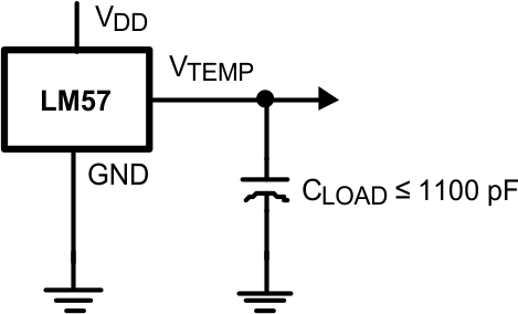 Figure 13. LM57 With No Isolation Resistor Required
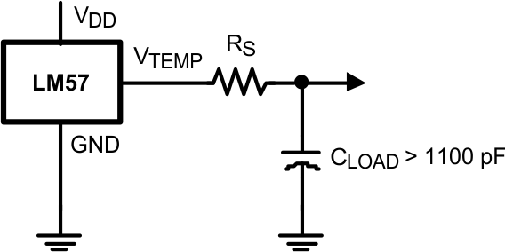 Figure 14. LM57 With Series Resistor for Capacitive Loading Greater than 1100 pF
Table 6. CLOAD and RS Values of Figure 14
| CLOAD | Minimum RS |
|---|---|
| 1.1 to 99 nF | 3 kΩ |
| 100 to 999 nF | 1.5 kΩ |
| 1 μF | 750 Ω |
8.3.6.3 VTEMP Voltage Shift
The LM57 is very linear over temperature and supply voltage range. Due to the intrinsic behavior of an NMOS/PMOS rail-to-rail buffer, a slight shift in the output can occur when the supply voltage is ramped over the operating range of the device. The location of the shift is determined by the relative levels of VDD and VTEMP. The shift typically occurs when VDD − VTEMP = 1 V.
This slight shift (a few millivolts) takes place over a wide change (approximately 200 mV) in VDD or VTEMP. Since the shift takes place over a wide temperature change of 5°C to 20°C, VTEMP is always monotonic. The accuracy specifications in the table already includes this possible shift.
8.4 Device Functional Modes
The LM57 has several modes of operation as detailed in the following drawings.
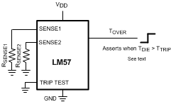 Figure 15. Temperature Switch Using Push-Pull Output
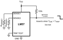 Figure 16. Temperature Switch Using Open-Drain Output
As shown in Figure 17 the LM57 has a TRIP Test input simplifying in situ board conductivity testing. Forcing TRIP TEST pin "HIGH" will drive the TOVER pin "LOW" and the TOVER pin "HIGH".
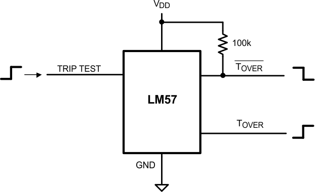 Figure 17. Trip Test Digital Output Test Circuit
In the circuit shown in Figure 18 when TOVER goes active high, it drives trip test high. Trip test high causes TOVER to stay high. It is therefore latched. To release the latch, power down, then power up. The LM57 always comes up in a released condition.
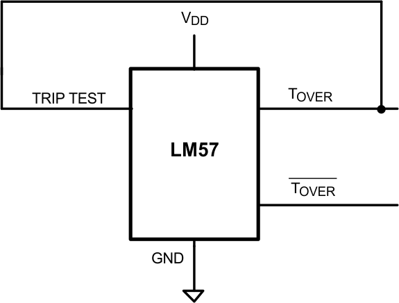 Figure 18. Simple Latch Circuit
The TRIP TEST pin, normally used to check the operation of the TOVER and TOVER pins, may be used to latch the outputs whenever the temperature exceeds the programmed limit and causes the digital outputs to assert. As shown in Figure 19, when TOVER goes high, the TRIP TEST input is also pulled high and causes TOVER output to latch high and the TOVER output to latch low. Momentarily switching the TRIP TEST input low will reset the LM57 to normal operation. The resistor limits the current out of the TOVER output pin.
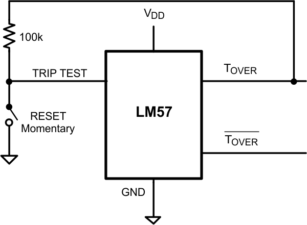 Figure 19. Latch Circuit Using TOVER Output