SNOS752E May 1999 – September 2014 LM6152 , LM6154
PRODUCTION DATA.
- 1Features
- 2Applications
- 3Description
- 4Revision History
- 5Pin Configuration and Functions
-
6Specifications
- 6.1 Absolute Maximum Ratings
- 6.2 Handling Ratings
- 6.3 Recommended Operating Conditions
- 6.4 Thermal Information
- 6.5 5.0 V DC Electrical Characteristics
- 6.6 5.0 V AC Electrical Characteristics
- 6.7 2.7 V DC Electrical Characteristics
- 6.8 2.7 V AC Electrical Characteristics
- 6.9 24 V DC Electrical Characteristics
- 6.10 24 V AC Electrical Characteristics
- 6.11 Typical Performance Characteristics
- 7Application and Implementation
- 8Device and Documentation Support
- 9Mechanical, Packaging, and Orderable Information
Package Options
Mechanical Data (Package|Pins)
- D|8
Thermal pad, mechanical data (Package|Pins)
Orderable Information
1 Features
- At VS = 5V, typical unless noted.
- Greater than Rail-to-rail Input CMVR −0.2 5V to 5.25 V
- Rail-to-rail Output Swing 0.01 V to 4.99 V
- Wide Gain-bandwidth 75 MHz @ 100 kHz
- Slew Rate
- Small Signal 5 V/µs
- Large Signal 45 V/µs
- Low Supply Current 1.4 mA/amplifier
- Wide Supply Range 2.7 V to 24 V
- Fast Settling Time of 1.1 µs for 2 V Step (to 0.01%)
- PSRR 91 dB
- CMRR 84 dB
2 Applications
- Portable High Speed Instrumentation
- Signal Conditioning Amplifier/ADC Buffers
- Barcode Scanners
3 Description
Using patented circuit topologies, the LM6152/LM6154 provides new levels of speed vs. power performance in applications where low voltage supplies or power limitations previously made compromise necessary. With only 1.4 mA/amplifier supply current, the 75 MHz gain bandwidth of this device supports new portable applications where higher power devices unacceptably drain battery life. The slew rate of the devices increases with increasing input differential voltage, thus allowing the device to handle capacitive loads while maintaining large signal amplitude.
The LM6152/LM6154 can be driven by voltages that exceed both power supply rails, thus eliminating concerns about exceeding the common-mode voltage range. The rail-to-rail output swing capability provides the maximum possible dynamic range at the output. This is particularly important when operating on low supply voltages.
Operating on supplies from 2.7 V to over 24 V, the LM6152/LM6154 is excellent for a very wide range of applications, from battery operated systems with large bandwidth requirements to high speed instrumentation.
Device Information(1)
| PART NUMBER | PACKAGE | BODY SIZE (NOM) |
|---|---|---|
| LM6152 | SOIC (8) | 4.902 mm × 3.912 mm |
| LM6154 | SOIC (14) | 8.636 mm × 3.912 mm |
- For all available packages, see the orderable addendum at the end of the datasheet.
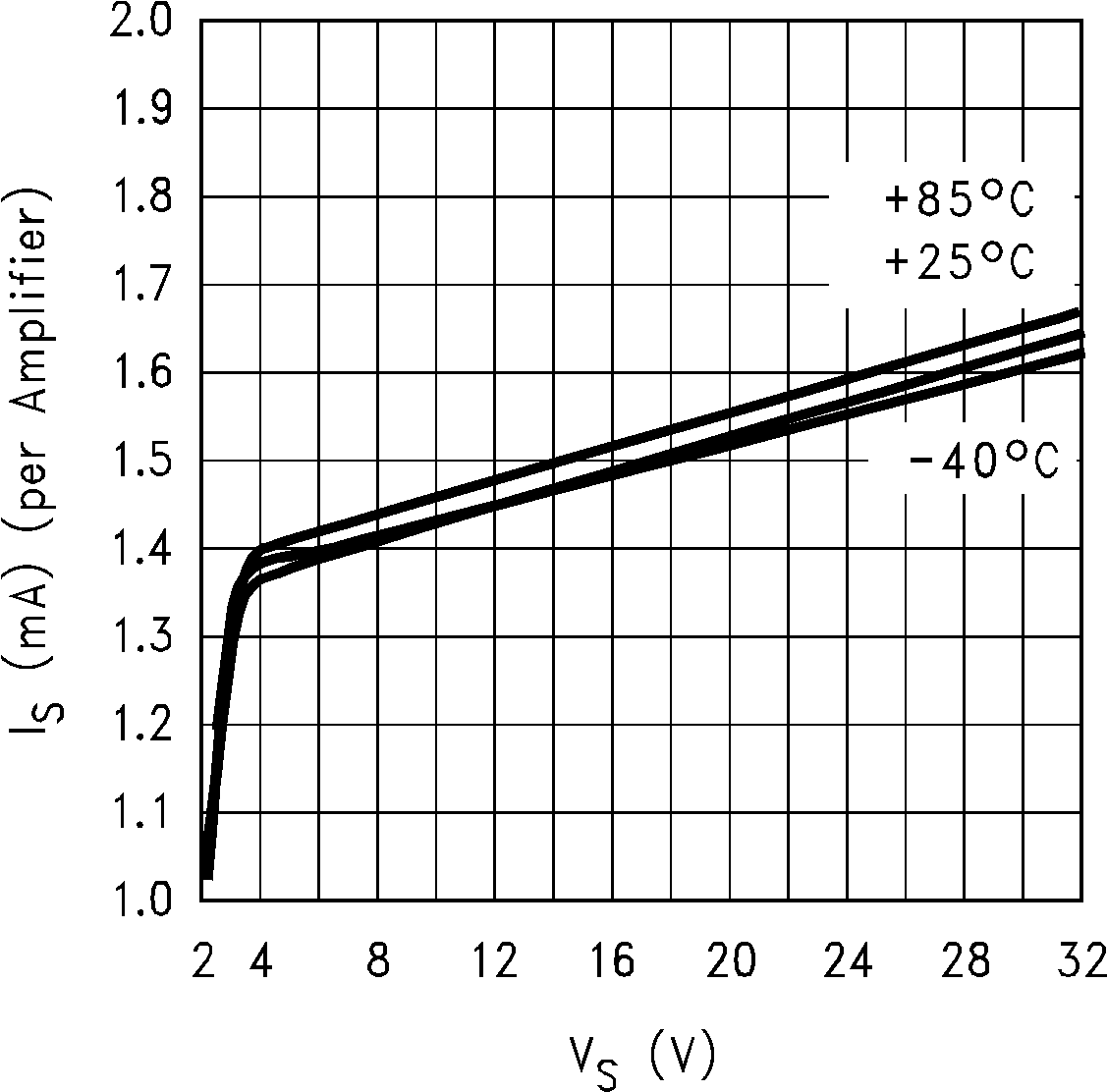
Supply Current vs. Supply Voltage
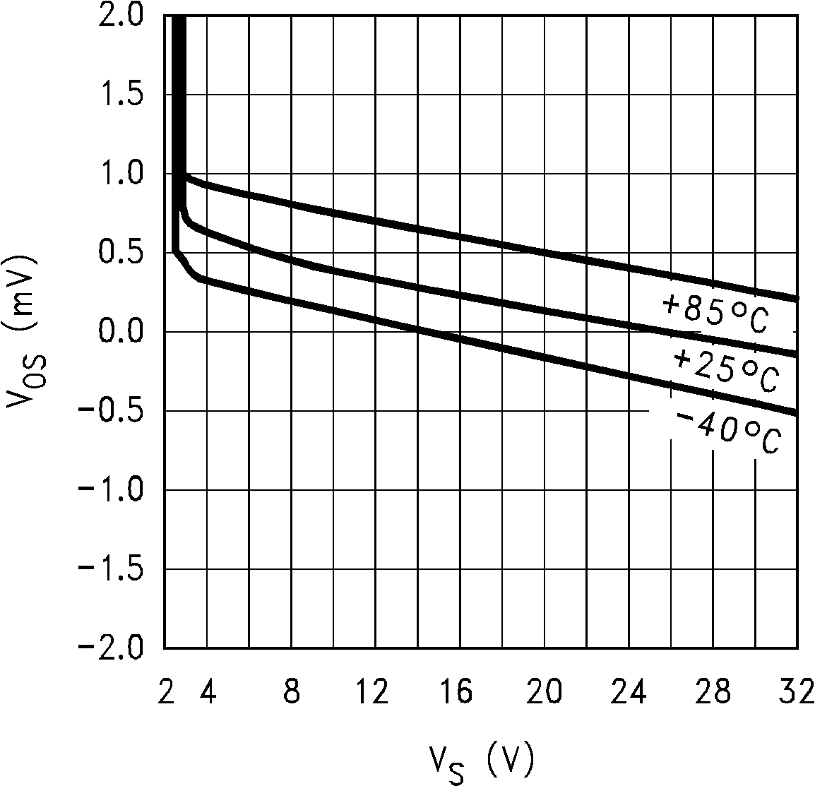
Offset Voltage vs. Supply voltage