SNOS469J April 2000 – January 2015 LM8261
PRODUCTION DATA.
- 1 Features
- 2 Applications
- 3 Description
- 4 Revision History
- 5 Pin Configuration and Functions
- 6 Specifications
- 7 Application and Implementation
- 8 Power Supply Recommendations
- 9 Layout
- 10Device and Documentation Support
- 11Mechanical, Packaging, and Orderable Information
Package Options
Mechanical Data (Package|Pins)
- DBV|5
Thermal pad, mechanical data (Package|Pins)
Orderable Information
7 Application and Implementation
7.1 Block Diagram and Operational Description
7.1.1 A) Input Stage
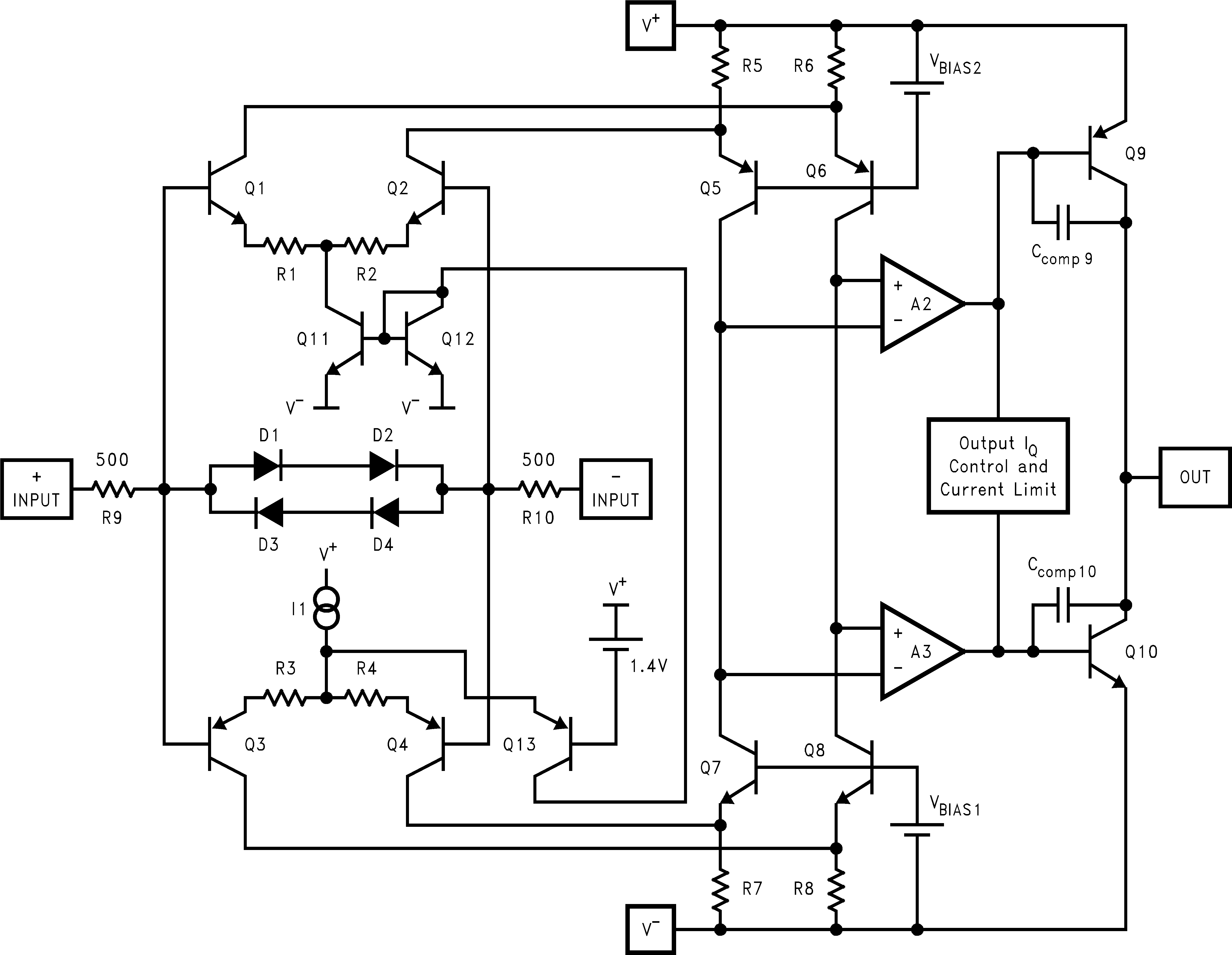 Figure 49. Simplified Schematic Diagram
As seen in Figure 49, the input stage consists of two distinct differential pairs (Q1-Q2 and Q3-Q4) in order to accommodate the full Rail-to-Rail input common mode voltage range. The voltage drop across R5, R6, R7, and R8 is kept to less than 200 mV in order to allow the input to exceed the supply rails. Q13 acts as a switch to steer current away from Q3-Q4 and into Q1-Q2, as the input increases beyond 1.4 V of V+. This in turn shifts the signal path from the bottom stage differential pair to the top one and causes a subsequent increase in the supply current.
In transitioning from one stage to another, certain input stage parameters (VOS, Ib, IOS, en, and in) are determined based on which differential pair is "on" at the time. Input Bias current, IB, will change in value and polarity as the input crosses the transition region. In addition, parameters such as PSRR and CMRR which involve the input offset voltage will also be effected by changes in VCM across the differential pair transition region.
The input stage is protected with the combination of R9-R10 and D1, D2, D3, and D4 against differential input over-voltages. This fault condition could otherwise harm the differential pairs or cause offset voltage shift in case of prolonged over voltage. As shown in Figure 50, if this voltage reaches approximately ±1.4 V at 25°C, the diodes turn on and current flow is limited by the internal series resistors (R9 and R10). The Absolute Maximum Rating of ±10 V differential on VIN still needs to be observed. With temperature variation, the point were the diodes turn on will change at the rate of 5 mV/°C.
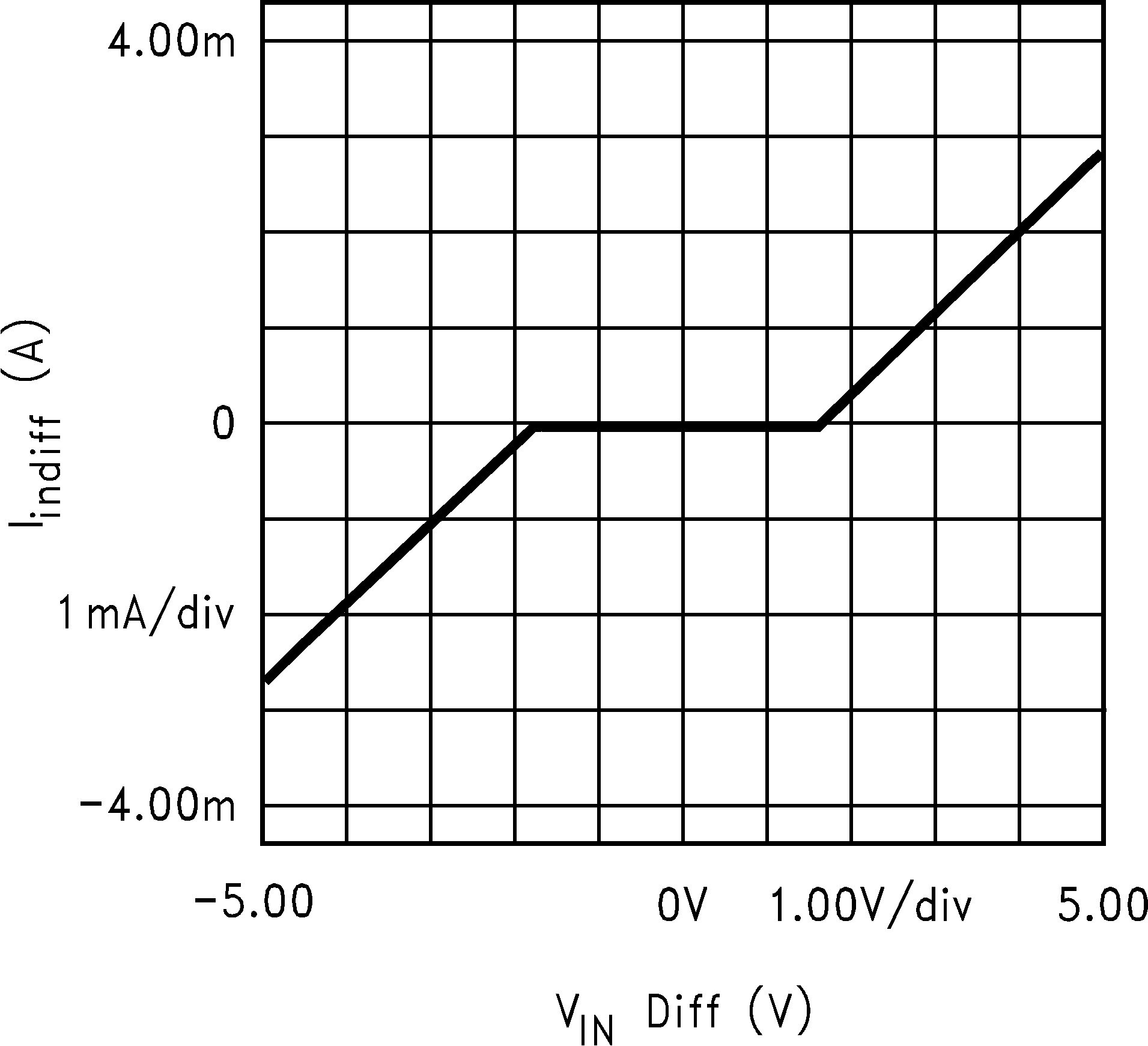 Figure 50. Input Stage Current vs. Differential Input Voltage
7.1.2 B) Output Stage
The output stage Figure 49 is comprised of complementary NPN and PNP common-emitter stages to permit voltage swing to within a VCE(SAT) of either supply rail. Q9 supplies the sourcing and Q10 supplies the sinking current load. Output current limiting is achieved by limiting the VCE of Q9 and Q10; using this approach to current limiting, alleviates the draw back to the conventional scheme which requires one VBE reduction in output swing.
The frequency compensation circuit includes Miller capacitors from collector to base of each output transistor (see Figure 49, Ccomp9 and Ccomp10). At light capacitive loads, the high frequency gain of the output transistors is high, and the Miller effect increases the effective value of the capacitors thereby stabilizing the Op Amp. Large capacitive loads greatly decrease the high frequency gain of the output transistors thus lowering the effective internal Miller capacitance - the internal pole frequency increases at the same time a low frequency pole is created at the Op Amp output due to the large load capacitor. In this fashion, the internal dominant pole compensation, which works by reducing the loop gain to less than 0dB when the phase shift around the feedback loop is more than 180°C, varies with the amount of capacitive load and becomes less dominant when the load capacitor has increased enough. Hence the Op Amp is very stable even at high values of load capacitance resulting in the uncharacteristic feature of stability under all capacitive loads.
7.2 Driving Capacitive Loads
The LM8261 is specifically designed to drive unlimited capacitive loads without oscillations (See Figure 30). In addition, the output current handling capability of the device allows for good slewing characteristics even with large capacitive loads (see Slew Rate vs. Cap Load plots, Figure 31 through Figure 34). The combination of these features is ideal for applications such as TFT flat panel buffers, A/D converter input amplifiers, and so forth.
However, as in most Op Amps, addition of a series isolation resistor between the Op Amp and the capacitive load improves the settling and overshoot performance.
Output current drive is an important parameter when driving capacitive loads. This parameter will determine how fast the output voltage can change. Referring to the Slew Rate vs. Cap Load Plots (Figure 31 through Figure 34), two distinct regions can be identified. Below about 10,000pF, the output Slew Rate is solely determined by the Op Amp's compensation capacitor value and available current into that capacitor. Beyond 10nF, the Slew Rate is determined by the Op Amp's available output current. Note that because of the lower output sourcing current compared to the sinking one, the Slew Rate limit under heavy capacitive loading is determined by the positive transitions. An estimate of positive and negative slew rates for loads larger than 100nF can be made by dividing the short circuit current value by the capacitor.
For the LM8261, the available output current increases with the input overdrive. As seen in Figure 51 and Figure 52, both sourcing and sinking short circuit current increase as input overdrive increases. In a closed loop amplifier configuration, during transient conditions while the fed back output has not quite caught up with the input, there will be an overdrive imposed on the input allowing more output current than would normally be available under steady state condition. Because of this feature, the Op Amp's output stage quiescent current can be kept to a minimum, thereby reducing power consumption, while enabling the device to deliver large output current when the need arises (such as during transients).
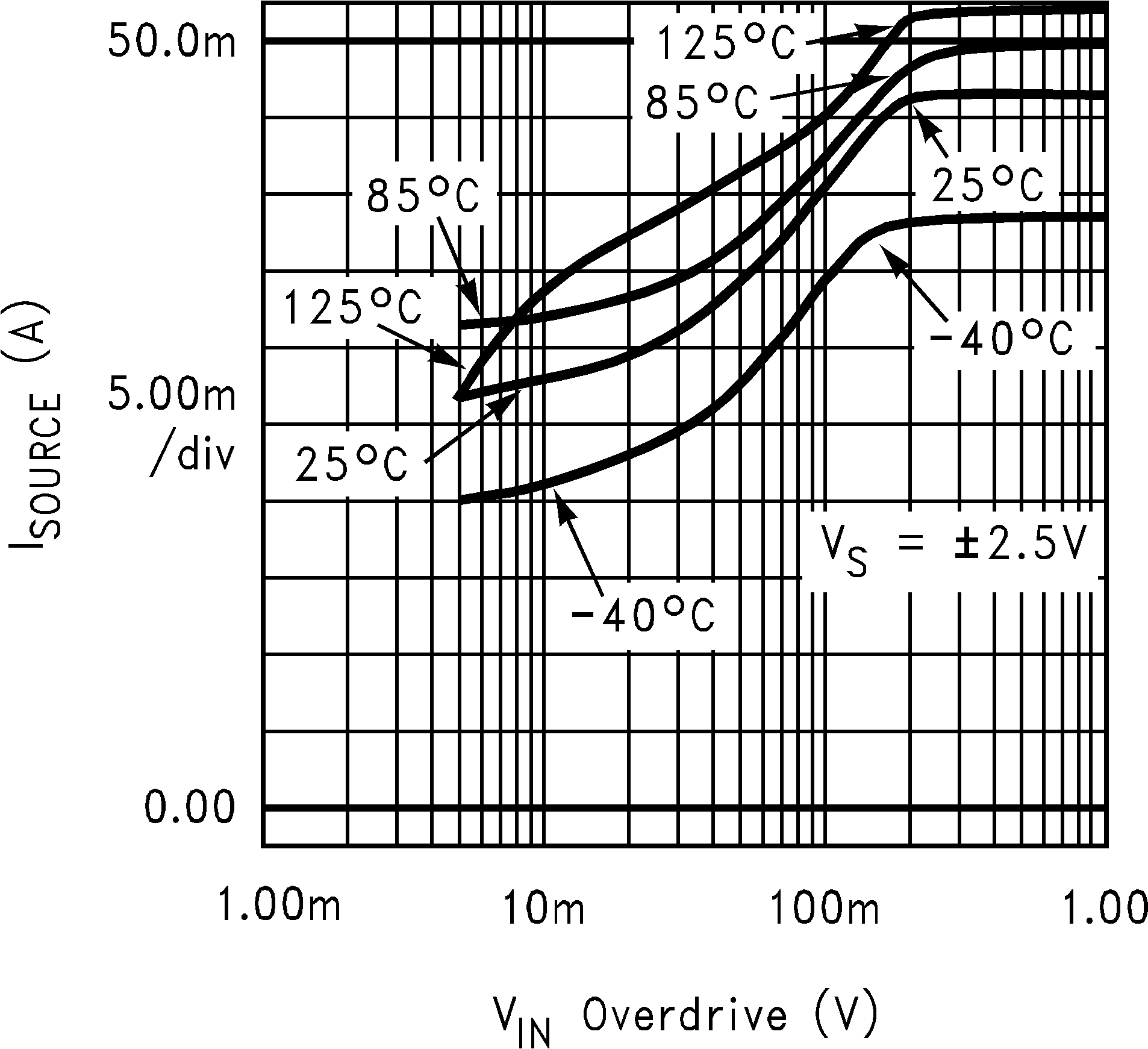 Figure 51. Output Short Circuit Sourcing Current vs. Input Overdrive
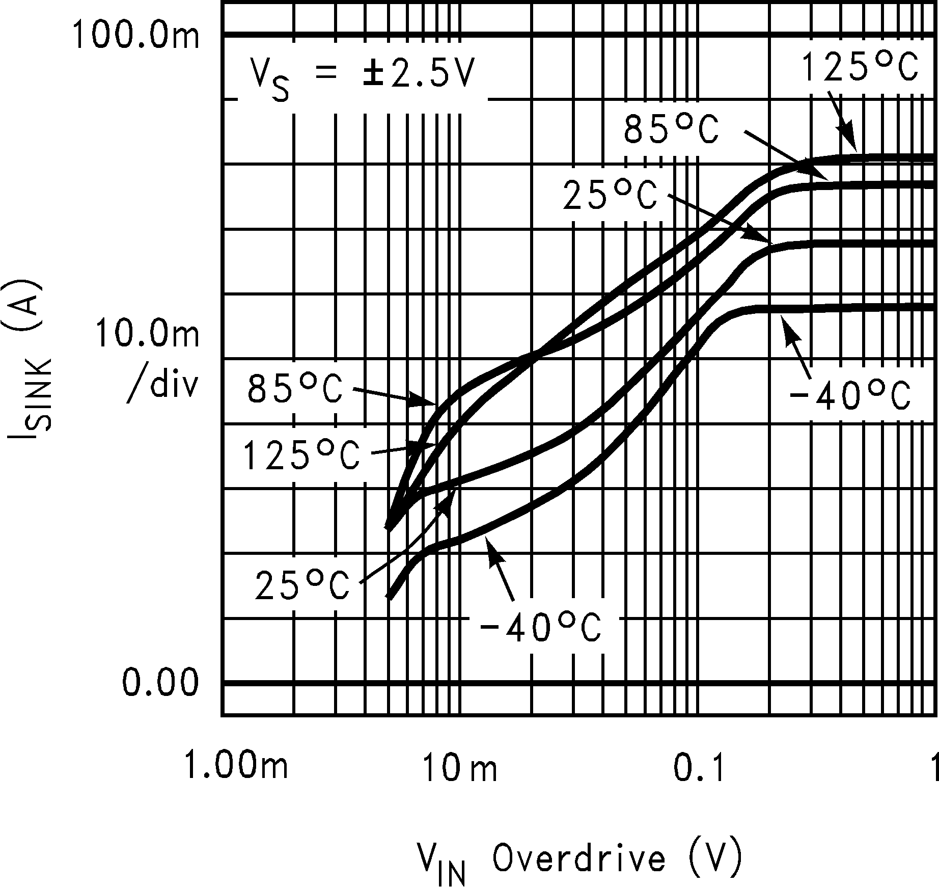 Figure 52. Output Short Circuit Sinking Current vs. Input Overdrive
Figure 53 shows the output voltage, output current, and the resulting input overdrive with the device set for AV = +1 and the input tied to a 1VPP step function driving a 47nF capacitor. During the output transition, the input overdrive reaches 1 V peak and is more than enough to cause the output current to increase to its maximum value (see Figure 51 and Figure 52). Because the larger output sinking current is compared to the sourcing one, the output negative transition is faster than the positive one.
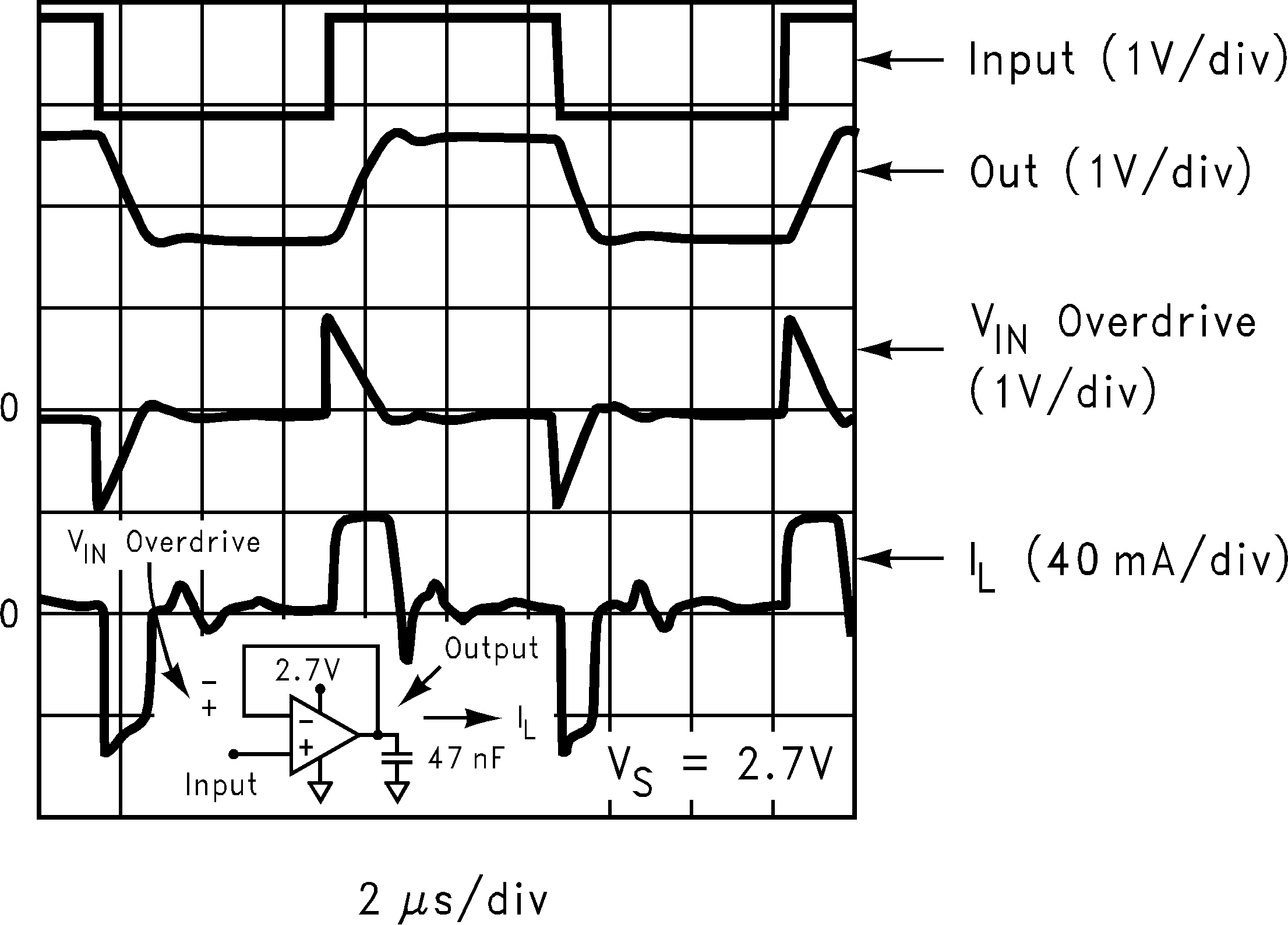 Figure 53. Buffer Amplifier Scope Photo
7.3 Estimating the Output Voltage Swing
It is important to keep in mind that the steady state output current will be less than the current available when there is an input overdrive present. For steady state conditions, Figure 24 through Figure 26 in Typical Characteristics can be used to predict the output swing. Figure 54 and Figure 55 show this performance along with several load lines corresponding to loads tied between the output and ground. In each cases, the intersection of the device plot at the appropriate temperature with the load line would be the typical output swing possible for that load. For example, a 1-KΩ load can accommodate an output swing to within 250 mV of V− and to 330 mV of V+ (VS = ±15 V) corresponding to a typical 29.3 VPP unclipped swing.
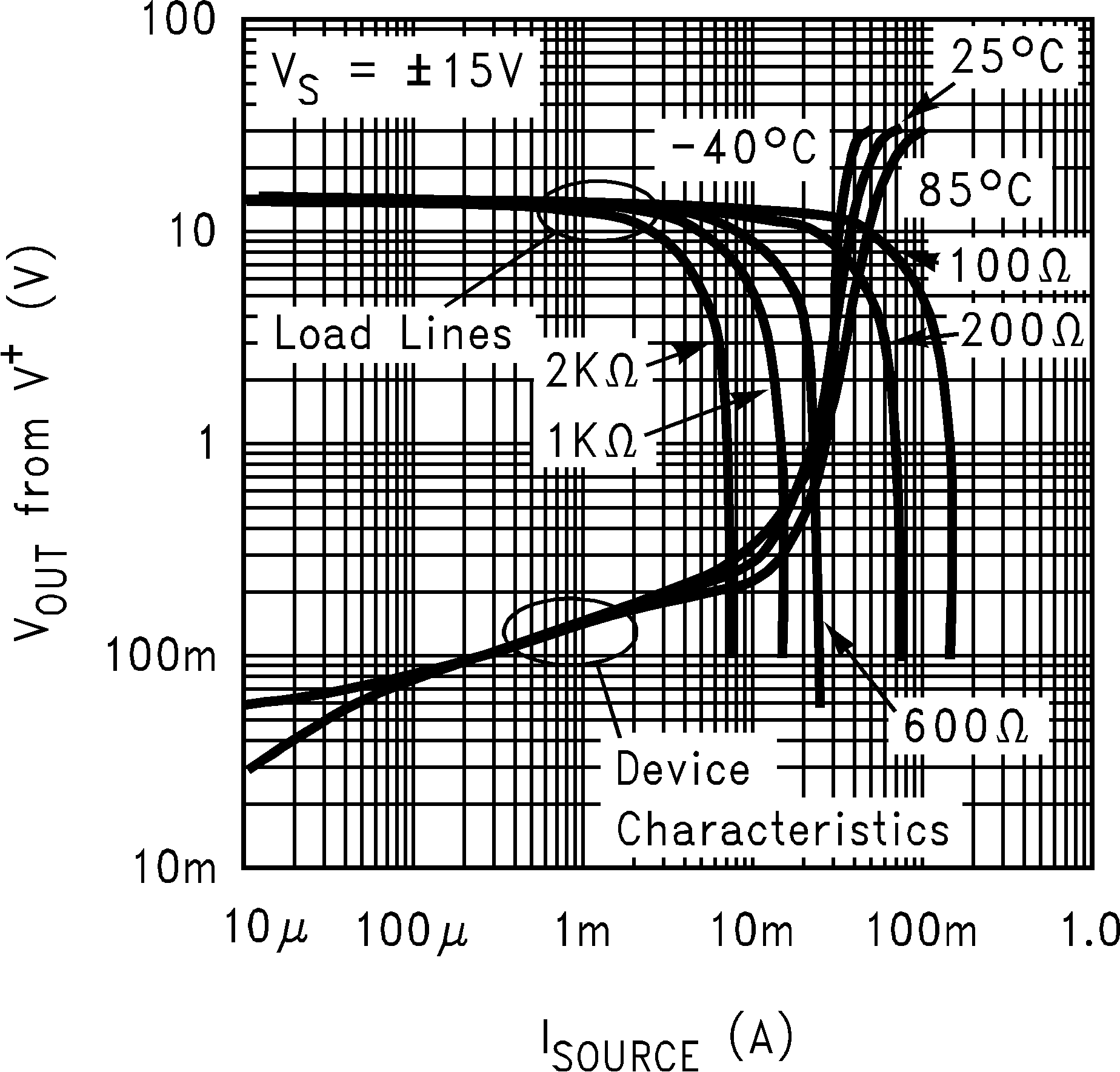 Figure 54. Output Sourcing Characteristics with Load Lines
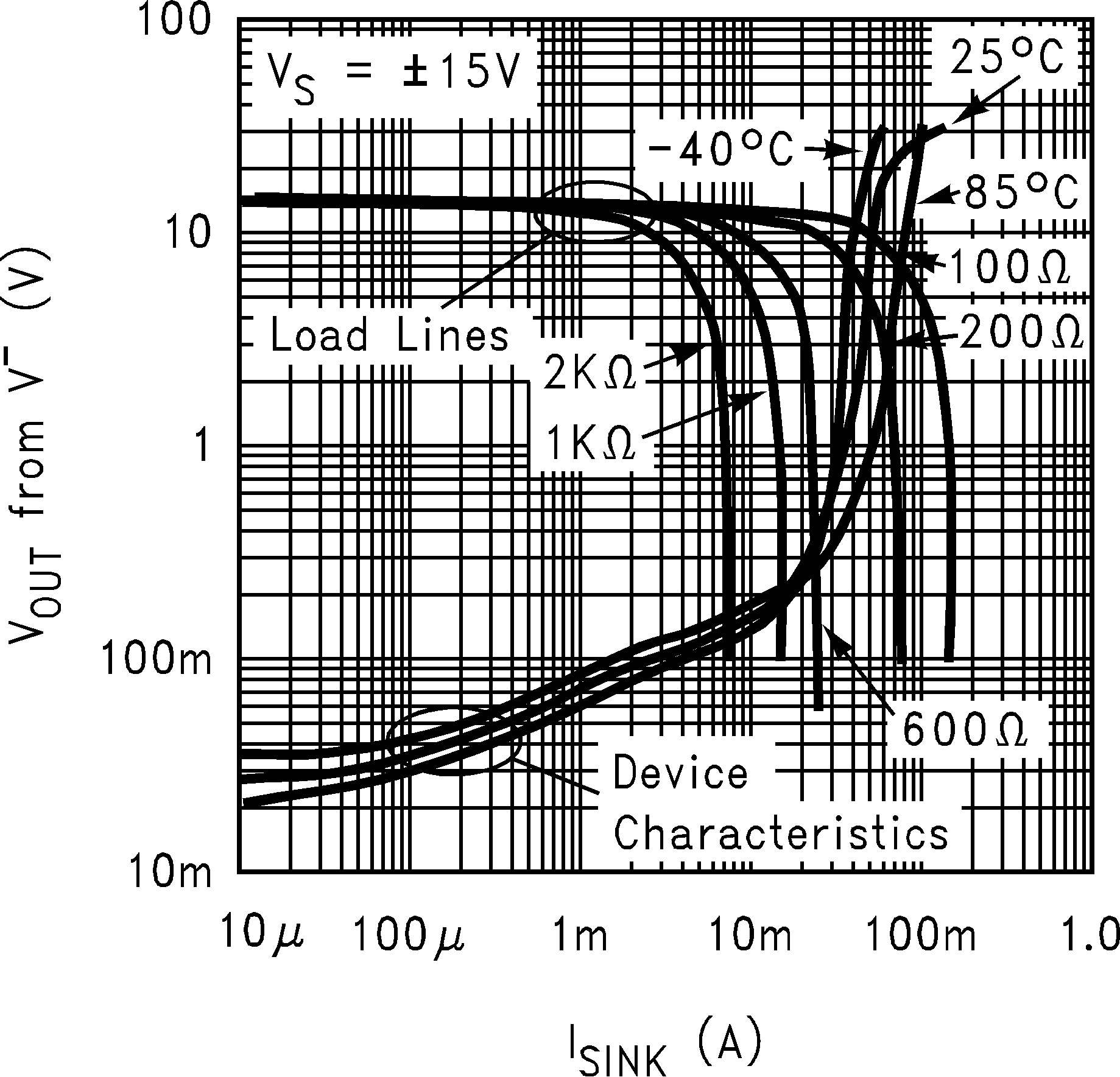 Figure 55. Output Sinking Characteristics with Load Lines
7.4 TFT Applications
Figure 56 below, shows a typical application where the LM8261 is used as a buffer amplifier for the VCOM signal employed in a TFT LCD flat panel:
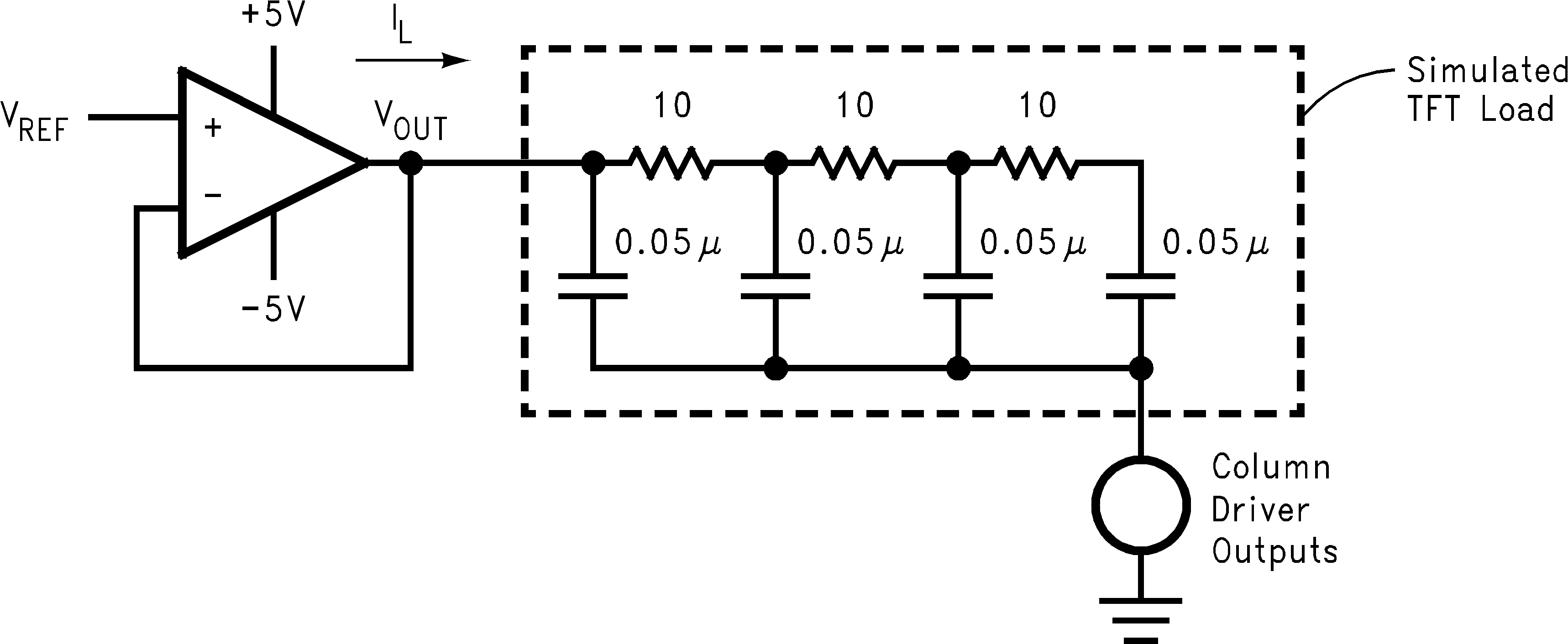 Figure 56. VCOM Driver Application Schematic
Figure 57 shows the time domain response of the amplifier when used as a VCOM buffer/driver with VREF at ground. In this application, the Op Amp loop will try and maintain its output voltage based on the voltage on its non-inverting input (VREF) despite the current injected into the TFT simulated load. As long as this load current is within the range tolerable by the LM8261 (45 mA sourcing and 65 mA sinking for ±5 V supplies), the output will settle to its final value within less than 2 µs.
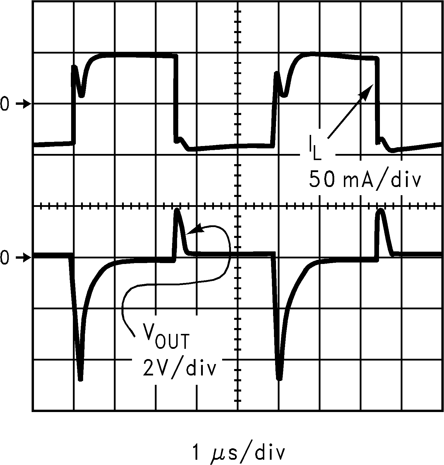 Figure 57. VCOM Driver Performance Scope Photo
7.5 Output Short Circuit Current and Dissipation Issues
The LM8261 output stage is designed for maximum output current capability. Even though momentary output shorts to ground and either supply can be tolerated at all operating voltages, longer lasting short conditions can cause the junction temperature to rise beyond the absolute maximum rating of the device, especially at higher supply voltage conditions. Below supply voltage of 6 V, output short circuit condition can be tolerated indefinitely.
With the Op Amp tied to a load, the device power dissipation consists of the quiescent power due to the supply current flow into the device, in addition to power dissipation due to the load current. The load portion of the power itself could include an average value (due to a DC load current) and an AC component. DC load current would flow if there is an output voltage offset, or the output AC average current is non-zero, or if the Op Amp operates in a single supply application where the output is maintained somewhere in the range of linear operation. Therefore:
Op Amp Quiescent Power Dissipation:
DC Load Power:
AC Load Power:
where
- IS is Supply Current
- VS is Total Supply Voltage (V+ - V−)
- IO is Average Load Current
- VO is Average Output Voltage
- VR is V+ for sourcing and V− for sinking current
Table 1 shows the maximum AC component of the load power dissipated by the Op Amp for standard Sinusoidal, Triangular, and Square Waveforms:
Table 1. Normalized AC Power Dissipated in the Output Stage for Standard Waveforms
| PAC (W.Ω/V2) | ||
|---|---|---|
| Sinusoidal | Triangular | Square |
| 50.7 x 10⁻³ | 46.9 x 10⁻³ | 62.5 x 10⁻³ |
The table entries are normalized to VS2/ RL. To calculate the AC load current component of power dissipation, simply multiply the table entry corresponding to the output waveform by the factor VS2/ RL. For example, with ±15 V supplies, a 600-Ω load, and triangular waveform power dissipation in the output stage is calculated as:
7.6 Other Application Hints
The use of supply decoupling is mandatory in most applications. As with most relatively high speed/high output current Op Amps, best results are achieved when each supply line is decoupled with two capacitors; a small value ceramic capacitor (∼0.01 µF) placed very close to the supply lead in addition to a large value Tantalum or Aluminum (> 4.7 µF). The large capacitor can be shared by more than one device if necessary. The small ceramic capacitor maintains low supply impedance at high frequencies while the large capacitor will act as the charge "bucket" for fast load current spikes at the Op Amp output. The combination of these capacitors will provide supply decoupling and will help keep the Op Amp oscillation free under any load.
7.6.1 LM8261 Advantages
Compared to other Rail-to-Rail Input/Output devices, the LM8261 offers several advantages such as:
- Improved cross over distortion.
- Nearly constant supply current throughout the output voltage swing range and close to either rail.
- Consistent stability performance for all input/output voltage and current conditions.
- Nearly constant Unity gain frequency (fu) and Phase Margin (Phim) for all operating supplies and load conditions.
- No output phase reversal under input overload condition.