SNIS140F May 2006 – September 2015 LM94022 , LM94022-Q1
PRODUCTION DATA.
- 1 Features
- 2 Applications
- 3 Description
- 4 Revision History
- 5 Pin Configuration and Functions
- 6 Specifications
- 7 Detailed Description
- 8 Application and Implementation
- 9 Power Supply Recommendations
- 10Layout
- 11Device and Documentation Support
- 12Mechanical, Packaging, and Orderable Information
Package Options
Mechanical Data (Package|Pins)
- DCK|5
Thermal pad, mechanical data (Package|Pins)
Orderable Information
10 Layout
10.1 Layout Guidelines
10.1.1 Mounting and Thermal Conductivity
The LM94022/-Q1 can be applied easily in the same way as other integrated-circuit temperature sensors. It can be glued or cemented to a surface.
To ensure good thermal conductivity, the backside of the LM94022/-Q1 die is directly attached to the GND pin (Pin 2). The temperatures of the lands and traces to the other leads of the LM94022/-Q1 will also affect the temperature reading.
Alternatively, the LM94022/-Q1 can be mounted inside a sealed-end metal tube, and can then be dipped into a bath or screwed into a threaded hole in a tank. As with any IC, the LM94022/-Q1 and accompanying wiring and circuits must be kept insulated and dry, to avoid leakage and corrosion. This is especially true if the circuit may operate at cold temperatures where condensation can occur. If moisture creates a short circuit from the output to ground or VDD, the output from the LM94022/-Q1 will not be correct. Printed-circuit coatings are often used to ensure that moisture cannot corrode the leads or circuit traces.
The thermal resistance junction to ambient (θJA) is the parameter used to calculate the rise of a device junction temperature due to its power dissipation. The equation used to calculate the rise in the die temperature of the LM94022/-Q1 is:

where
- TA is the ambient temperature,
- IQ is the quiescent current,
- ILis the load current on the output,
- and VO is the output voltage.
For example, in an application where TA = 30 °C, VDD = 5 V, IDD = 9 μA, Gain Select = 11, VOUT = 2.231 mV, and IL = 2 μA, the junction temperature would be 30.021 °C, showing a self-heating error of only 0.021°C. Because the junction temperature of the LM94022 is the actual temperature being measured, take care to minimize the load current that the LM94022/-Q1 is required to drive. Table 3 shows the thermal resistance of the LM94022/-Q1.
Table 3. LM94022/LM94022-Q1 Thermal Resistance
| DEVICE NUMBER | NS PACKAGE NUMBER | THERMAL RESISTANCE (θJA) |
|---|---|---|
| LM94022BIMG | DCK0005A | 415°C/W |
10.2 Layout Example
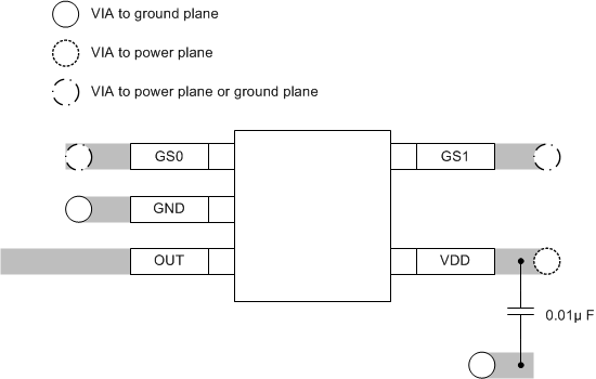
The LM94022/-Q1 is extremely simple to layout electrically. If a power supply bypass capacitor is used it should be connected as shown in Figure 20. The device pins and layout greatly influence the temperature that the LM94022/-Q1 die is measuring thus thermal modeling is recommended to ensure that the device is sensing the proper temperature.
 Figure 20. Recommended Layout
10.3 Output and Noise Considerations
A push-pull output gives the LM94022/-Q1 the ability to sink and source significant current. This is beneficial when, for example, driving dynamic loads like an input stage on an analog-to-digital converter (ADC). In these applications the source current is required to quickly charge the input capacitor of the ADC. See the Application Circuits section for more discussion of this topic. The LM94022/-Q1 is ideal for this and other applications which require strong source or sink current.
The supply-noise gain of the LM94022 (the ratio of the AC signal on VOUT to the AC signal on VDD) was measured during bench tests. It is typical attenuation is shown in the Typical Characteristics section. A load capacitor on the output can help to filter noise.
For operation in very noisy environments, some bypass capacitance should be present on the supply within approximately 2 inches of the LM94022/-Q1.