SNIS140F May 2006 – September 2015 LM94022 , LM94022-Q1
PRODUCTION DATA.
- 1 Features
- 2 Applications
- 3 Description
- 4 Revision History
- 5 Pin Configuration and Functions
- 6 Specifications
- 7 Detailed Description
- 8 Application and Implementation
- 9 Power Supply Recommendations
- 10Layout
- 11Device and Documentation Support
- 12Mechanical, Packaging, and Orderable Information
Package Options
Mechanical Data (Package|Pins)
- DCK|5
Thermal pad, mechanical data (Package|Pins)
Orderable Information
6 Specifications
6.1 Absolute Maximum Ratings
over operating free-air temperature range (unless otherwise noted)(1)(3)| MIN | MAX | UNIT | ||
|---|---|---|---|---|
| Supply Voltage | −0.3 | 6 | V | |
| Voltage at Output Pin | −0.3 | (VDD + 0.5) | V | |
| Output Current | ±7 | mA | ||
| Voltage at GS0 and GS1 Input Pins | −0.3 | 6 | V | |
| Input Current at any pin(2) | 5 | mA | ||
| Maximum Junction Temperature, TJMAX | 150 | °C | ||
| Storage temperature, Tstg | −65 | 150 | °C | |
(1) Stresses beyond those listed under Absolute Maximum Ratings may cause permanent damage to the device. These are stress ratings only, which do not imply functional operation of the device at these or any other conditions beyond those indicated under Recommended Operating Conditions. Exposure to absolute-maximum-rated conditions for extended periods may affect device reliability.
(2) When the input voltage (VI) at any pin exceeds power supplies (VI < GND or VI > V+), the current at that pin should be limited to 5 mA.
(3) Soldering process must comply with Reflow Temperature Profile specifications. Refer to http://www.ti.com/packaging
6.2 ESD Ratings
| VALUE | UNIT | |||
|---|---|---|---|---|
| V(ESD) | Electrostatic discharge | Human body model (HBM)(1)(2) | ±2500 | V |
| Machine model(2) | ±250 | |||
(1) JEDEC document JEP155 states that 500-V HBM allows safe manufacturing with a standard ESD control process.
(2) The human body model is a 100-pF capacitor discharged through a 1.5-kΩ resistor into each pin. The machine model is a 200-pF capacitor discharged directly into each pin.
6.3 Recommended Operating Conditions
over operating free-air temperature range (unless otherwise noted)(1)| MIN | MAX | UNIT | ||
|---|---|---|---|---|
| Free Air or Specified Temperature (TMIN ≤ TA ≤ TMAX) |
−50 | 150 | °C | |
| Supply Voltage (VDD) | 1.5 | 5.5 | V | |
(1) Absolute Maximum Ratings indicate limits beyond which damage to the device may occur. Operating Ratings indicate conditions for which the device is functional, but do not guarantee specific performance limits. For guaranteed specifications and test conditions, see the Electrical Characteristics. The guaranteed specifications apply only for the test conditions listed. Some performance characteristics may degrade when the device is not operated under the listed test conditions.
6.4 Thermal Information
| THERMAL METRIC(1) | LM94022, LM94022-Q1 | UNIT | |
|---|---|---|---|
| DCK (SC70) | |||
| 5 PINS | |||
| RθJA | Junction-to-ambient thermal resistance | 415 | °C/W |
(1) For more information about traditional and new thermal metrics, see the Semiconductor and IC Package Thermal Metrics application report, SPRA953.
6.5 Electrical Characteristics
Unless otherwise noted, these specifications apply for VDD = 1.5 V to 5.5 V; all limits TA = TJ = 25°C unless otherwise specified. These limits do not include DC load regulation. These stated accuracy limits are with reference to the values in the Table 2.| PARAMETER | CONDITIONS | MIN | TYP(1) | MAX(2) | UNIT | ||
|---|---|---|---|---|---|---|---|
| ACCURACY CHARACTERISTICS | |||||||
| Temperature Error(7) | GS1 = 0 GS0 = 0 |
TA = +20°C to +40°C; VDD = 1.5 V to 5.5 V |
–1.5 | 1.5 | °C | ||
| TA = +0°C to +70°C; VDD = 1.5 V to 5.5 V |
–1.8 | 1.8 | °C | ||||
| TA = +0°C to +90°C; VDD = 1.5 V to 5.5 V |
–2.1 | 2.1 | °C | ||||
| TA = +0°C to +120°C; VDD = 1.5 V to 5.5 V |
–2.4 | 2.4 | °C | ||||
| TA = +0°C to +150°C; VDD = 1.5 V to 5.5 V |
–2.7 | 2.7 | °C | ||||
| TA = −50°C to +0°C; VDD = 1.6 V to 5.5 V |
–1.8 | 1.8 | °C | ||||
| GS1 = 0 GS0 = 1 |
TA = +20°C to +40°C; VDD = 1.8 V to 5.5 V |
–1.5 | 1.5 | °C | |||
| TA = +0°C to +70°C; VDD = 1.9 V to 5.5 V |
–1.8 | 1.8 | °C | ||||
| TA = +0°C to +90°C; VDD = 1.9 V to 5.5 V |
–2.1 | 2.1 | °C | ||||
| TA = +0°C to +120°C; VDD = 1.9 V to 5.5 V |
–2.4 | 2.4 | °C | ||||
| TA = +0°C to +150°C; VDD = 1.9 V to 5.5 V |
–2.7 | 2.7 | °C | ||||
| TA = −50°C to +0°C; VDD = 2.3 V to 5.5 V |
–1.8 | 1.8 | °C | ||||
| GS1 = 1 GS0 = 0 |
TA = +20°C to +40°C; VDD = 2.2 V to 5.5 V |
–1.5 | 1.5 | °C | |||
| TA = +0°C to +70°C; VDD = 2.4 V to 5.5 V |
–1.8 | 1.8 | °C | ||||
| TA = +0°C to +90°C; VDD = 2.4 V to 5.5 V |
–2.1 | 2.1 | °C | ||||
| TA = +0°C to +120°C; VDD = 2.4 V to 5.5 V |
–2.4 | 2.4 | °C | ||||
| TA = +0°C to +150°C; VDD = 2.4 V to 5.5 V |
–2.7 | 2.7 | °C | ||||
| TA = −50°C to +0°C; VDD = 3.0 V to 5.5 V |
–1.8 | 1.8 | °C | ||||
| GS1 = 1 GS0 = 1 |
TA = +20°C to +40°C; VDD = 2.7 V to 5.5 V |
–1.5 | 1.5 | °C | |||
| TA = +0°C to +70°C; VDD = 3.0 V to 5.5 V |
–1.8 | 1.8 | °C | ||||
| TA = +0°C to +90°C; VDD = 3.0 V to 5.5 V |
–2.1 | 2.1 | °C | ||||
| TA = +0°C to +120°C; VDD = 3.0 V to 5.5 V |
–2.4 | 2.4 | °C | ||||
| TA = 0°C to +150°C; VDD = 3.0 V to 5.5 V |
–2.7 | 2.7 | °C | ||||
| TA = −50°C to +0°C; VDD = 3.6 V to 5.5 V |
–1.8 | 1.8 | °C | ||||
| Sensor Gain | GS1 = 0, GS0 = 0 | –5.5 | mV/°C | ||||
| GS1 = 0, GS0 = 1 | –8.2 | mV/°C | |||||
| GS1 = 1, GS0 = 0 | –10.9 | mV/°C | |||||
| GS1 = 1, GS0 = 1 | –13.6 | mV/°C | |||||
| Load Regulation(3) | Source ≤ 50 μA, (VDD – VOUT) ≥ 200 mV |
–0.22 | mV | ||||
| TA = TJ = TMIN to TMAX | –1 | ||||||
| Sink ≤ 50 μA, VOUT ≥ 200 mV |
0.26 | mV | |||||
| TA = TJ = TMIN to TMAX | 1 | ||||||
| Line Regulation(4) | 200 | μV/V | |||||
| IS | Supply Current | (VDD – VOUT) ≥ 100 mV | 5.4 | μA | |||
| TA = TJ = +30°C to +150°C | 8.1 | ||||||
| (VDD – VOUT) ≥ 100 mV | 5.4 | μA | |||||
| TA = TJ = TMIN to TMAX | 9 | ||||||
| CL | Output Load Capacitance | 1100 | pF | ||||
| Power-ON Time(5) | CL= 0 pF to 1100 pF | 0.7 | ms | ||||
| TA = TJ = TMIN to TMAX | 1.9 | ||||||
| VIH | GS1 and GS0 Input Logic 1 Threshold Voltage | TA = TJ = TMIN to TMAX | VDD – 0.5 | V | |||
| VIL | GS1 and GS0 Input Logic 0 Threshold Voltage | TA = TJ = TMIN to TMAX | 0.5 | V | |||
| IIH | Logic 1 Input Current(6) | 0.001 | μA | ||||
| TA = TJ = TMIN to TMAX | 1 | ||||||
| IIL | Logic 0 Input Current(6) | 0.001 | μA | ||||
| TA = TJ = TMIN to TMAX | 1 | ||||||
(1) Typicals are at TJ = TA = 25°C and represent most likely parametric norm.
(2) Limits are warrantied to TI's AOQL (Average Outgoing Quality Level).
(3) Source currents are flowing out of the LM94022/-Q1. Sink currents are flowing into the LM94022/-Q1.
(4) Line regulation (DC) is calculated by subtracting the output voltage at the highest supply voltage from the output voltage at the lowest supply voltage. The typical DC line regulation specification does not include the output voltage shift discussed in Output Voltage Shift.
(5) Warrantied by design and characterization.
(6) The input current is leakage only and is highest at high temperature. It is typically only 0.001 µA. The 1-µA limit is solely based on a testing limitation and does not reflect the actual performance of the part.
(7) Accuracy is defined as the error between the measured and reference output voltages, tabulated in the Transfer Table at the specified conditions of supply gain setting, voltage, and temperature (expressed in °C). Accuracy limits include line regulation within the specified conditions. Accuracy limits do not include load regulation; they assume no DC load.
6.6 Typical Characteristics
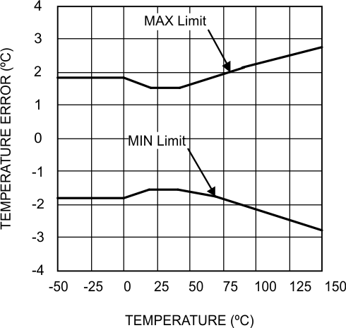 Figure 1. Temperature Error vs. Temperature
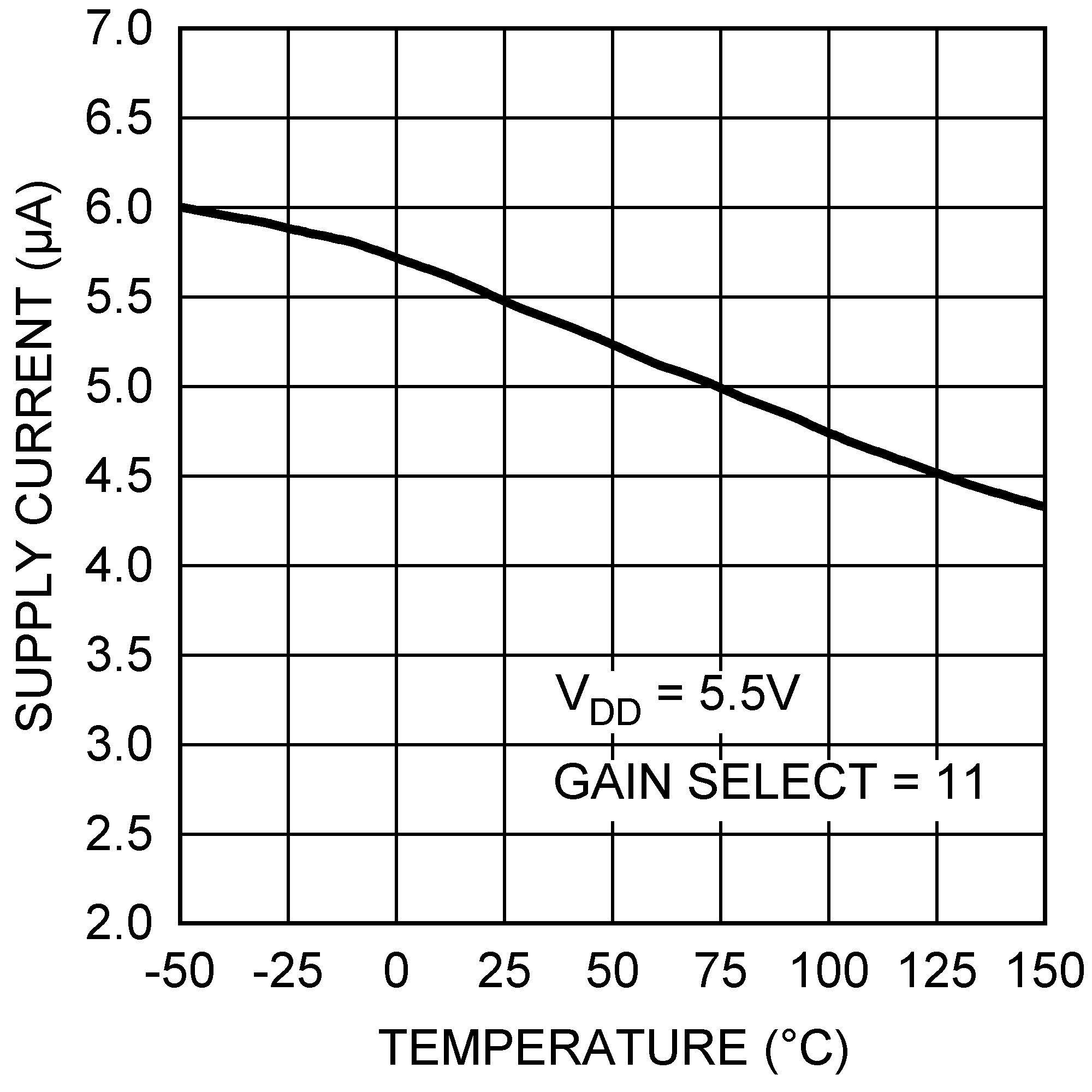 Figure 3. Supply Current vs. Temperature
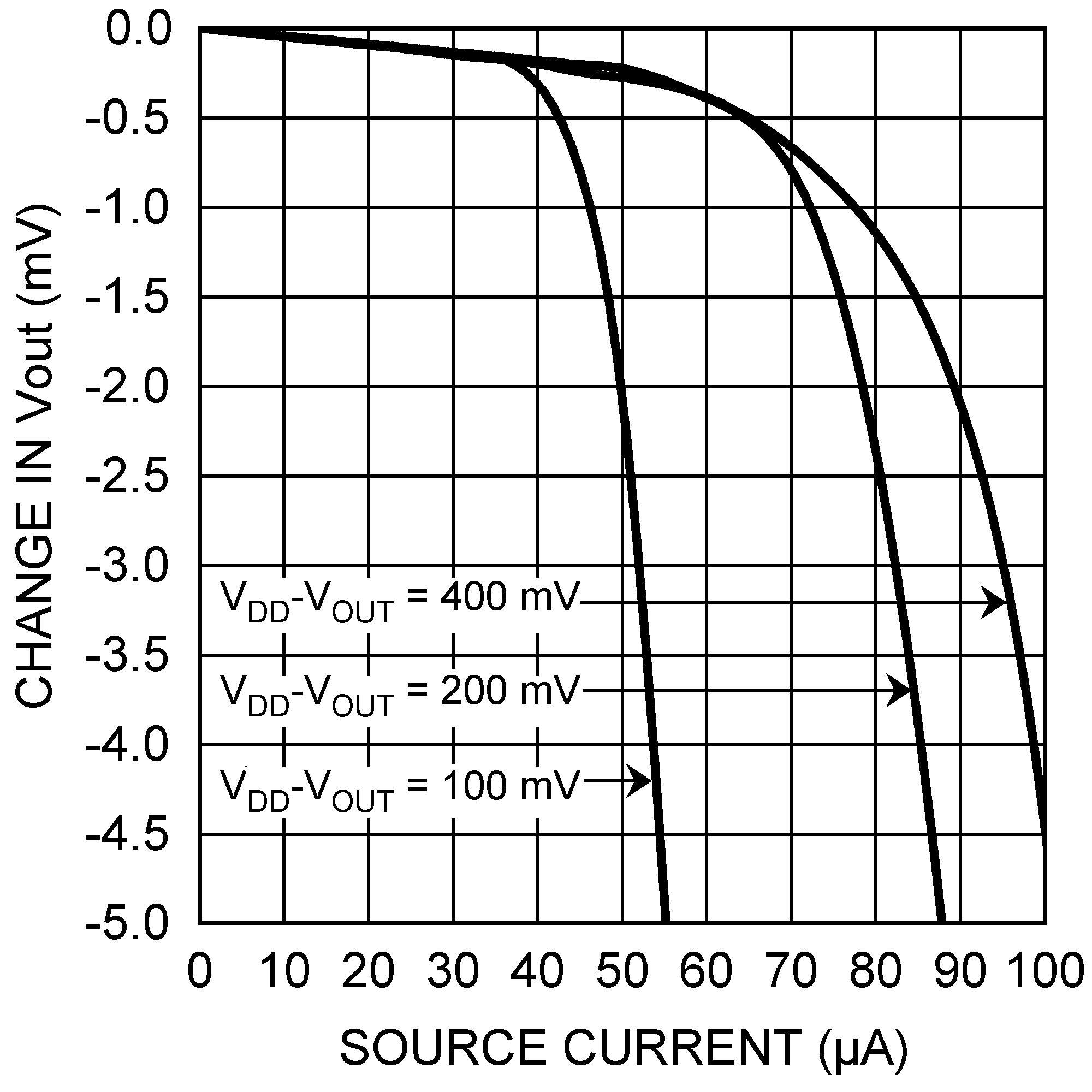 Figure 5. Load Regulation, Sourcing Current
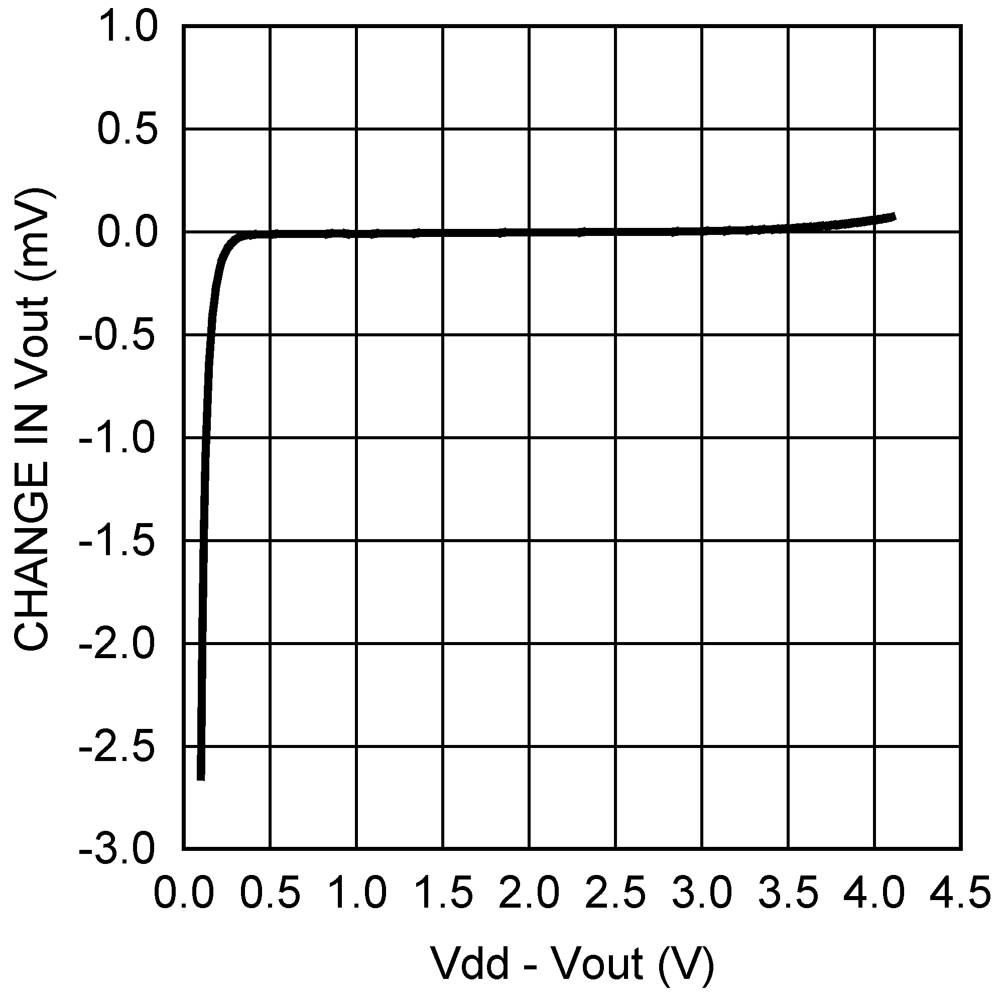 Figure 7. Change in Vout vs. Overhead Voltage
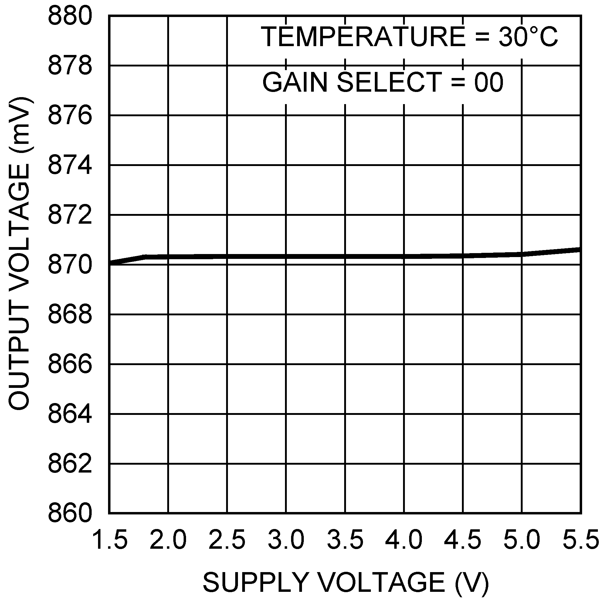 Figure 9. Output Voltage vs. Supply Voltage
 Gain Select = 00
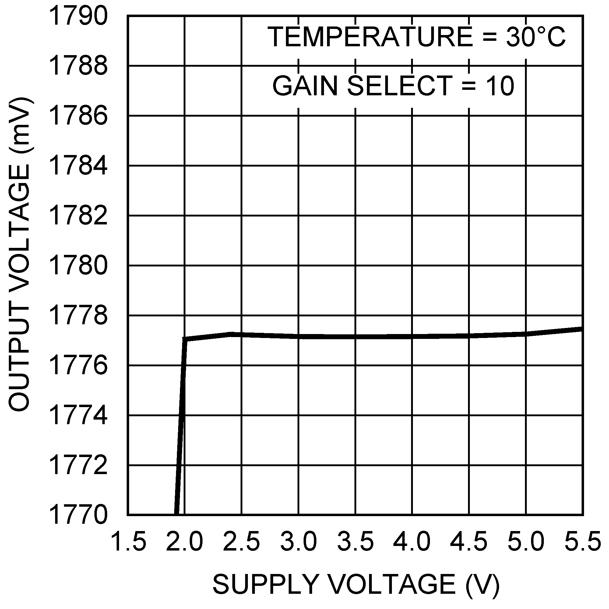 Figure 11. Output Voltage vs. Supply Voltage
 Gain Select = 10
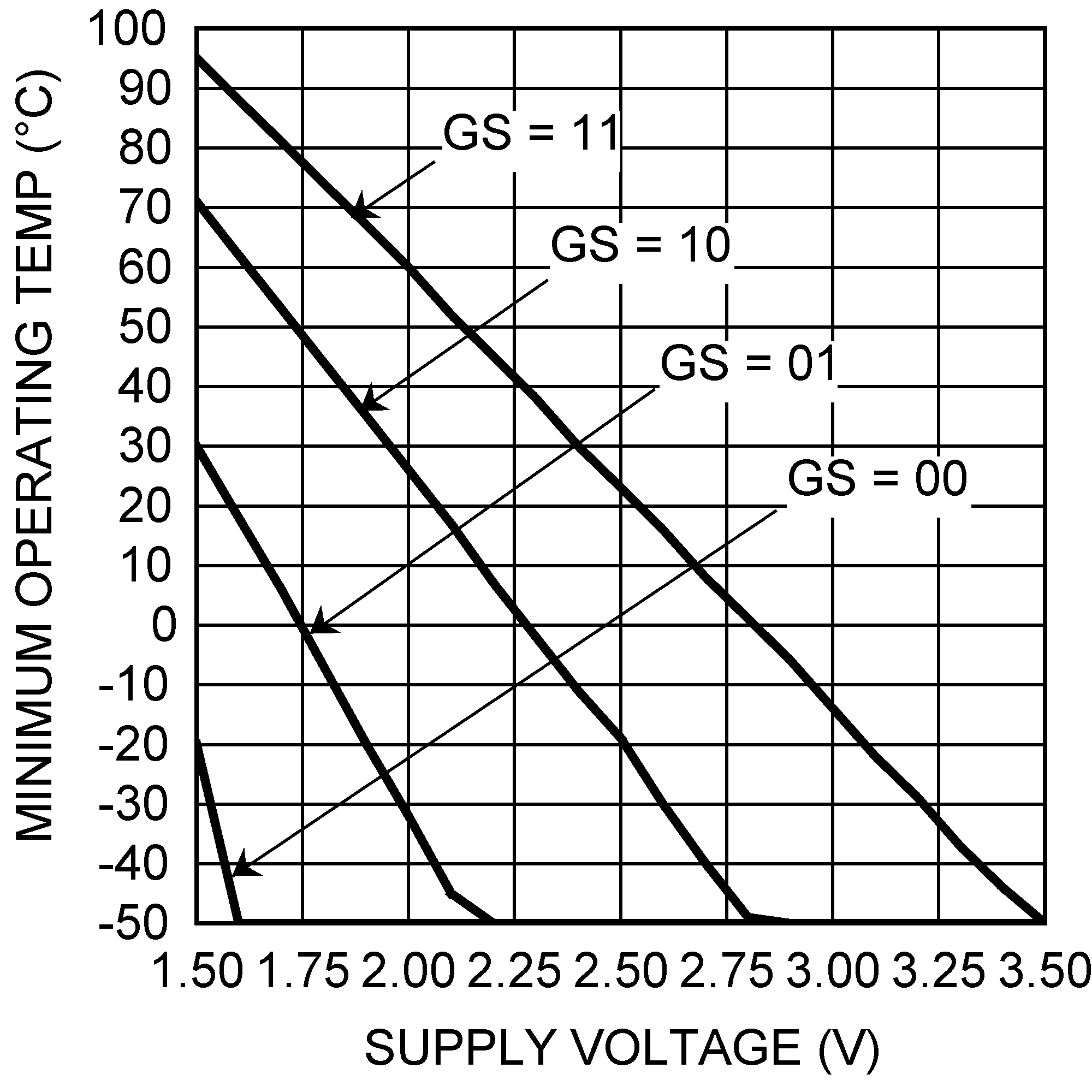 Figure 2. Minimum Operating Temperature vs. Supply Voltage
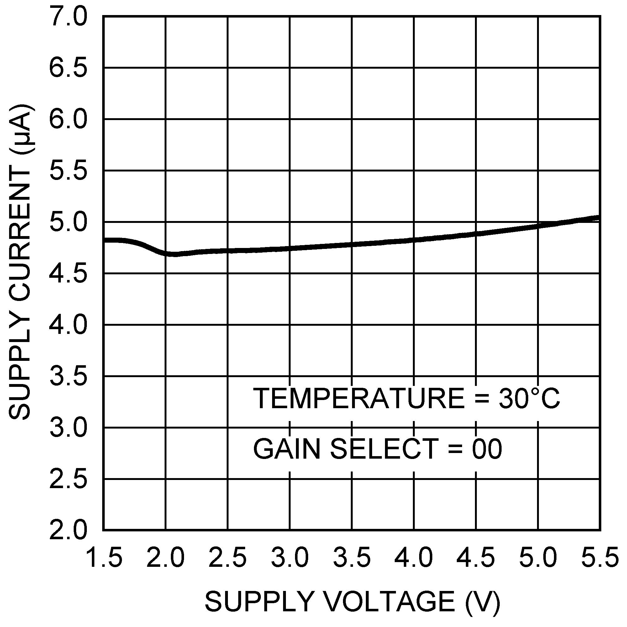 Figure 4. Supply Current vs. Supply Voltage
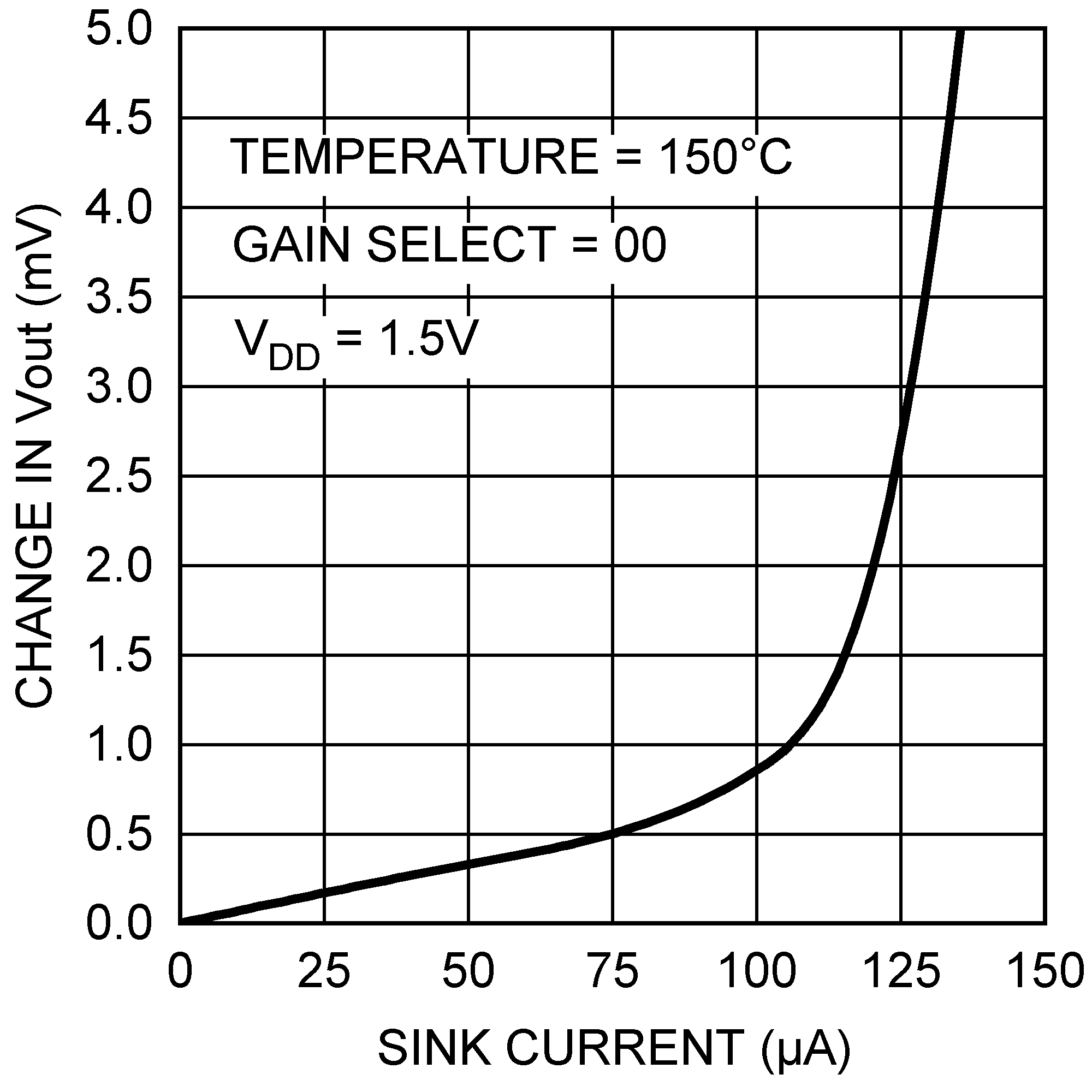 Figure 6. Load Regulation, Sinking Current
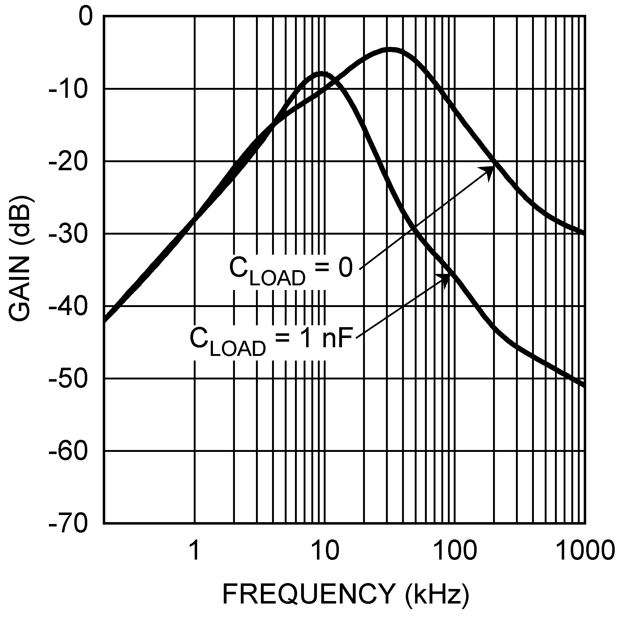 Figure 8. Supply-Noise Gain vs. Frequency
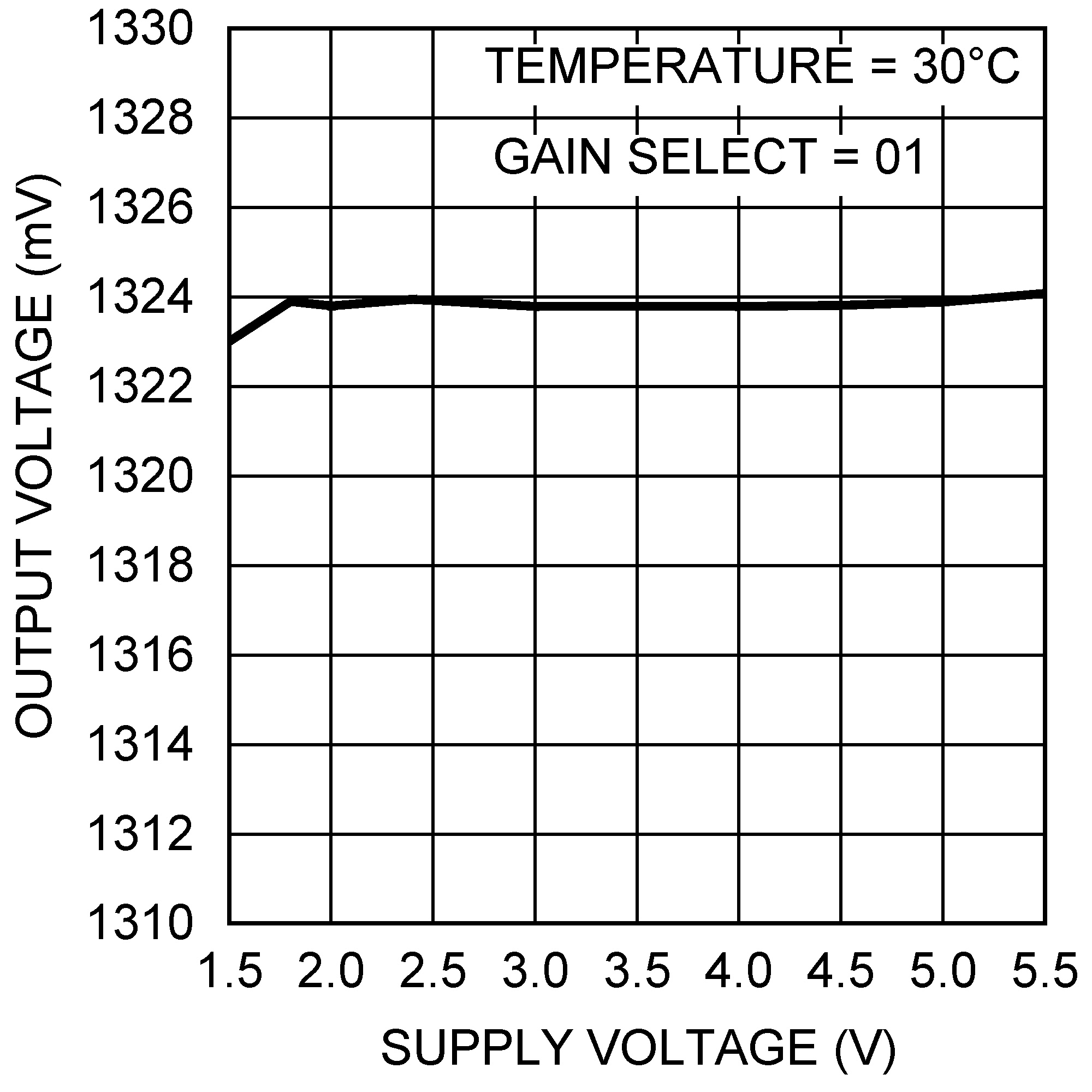 Figure 10. Output Voltage vs. Supply Voltage
 Gain Select = 01
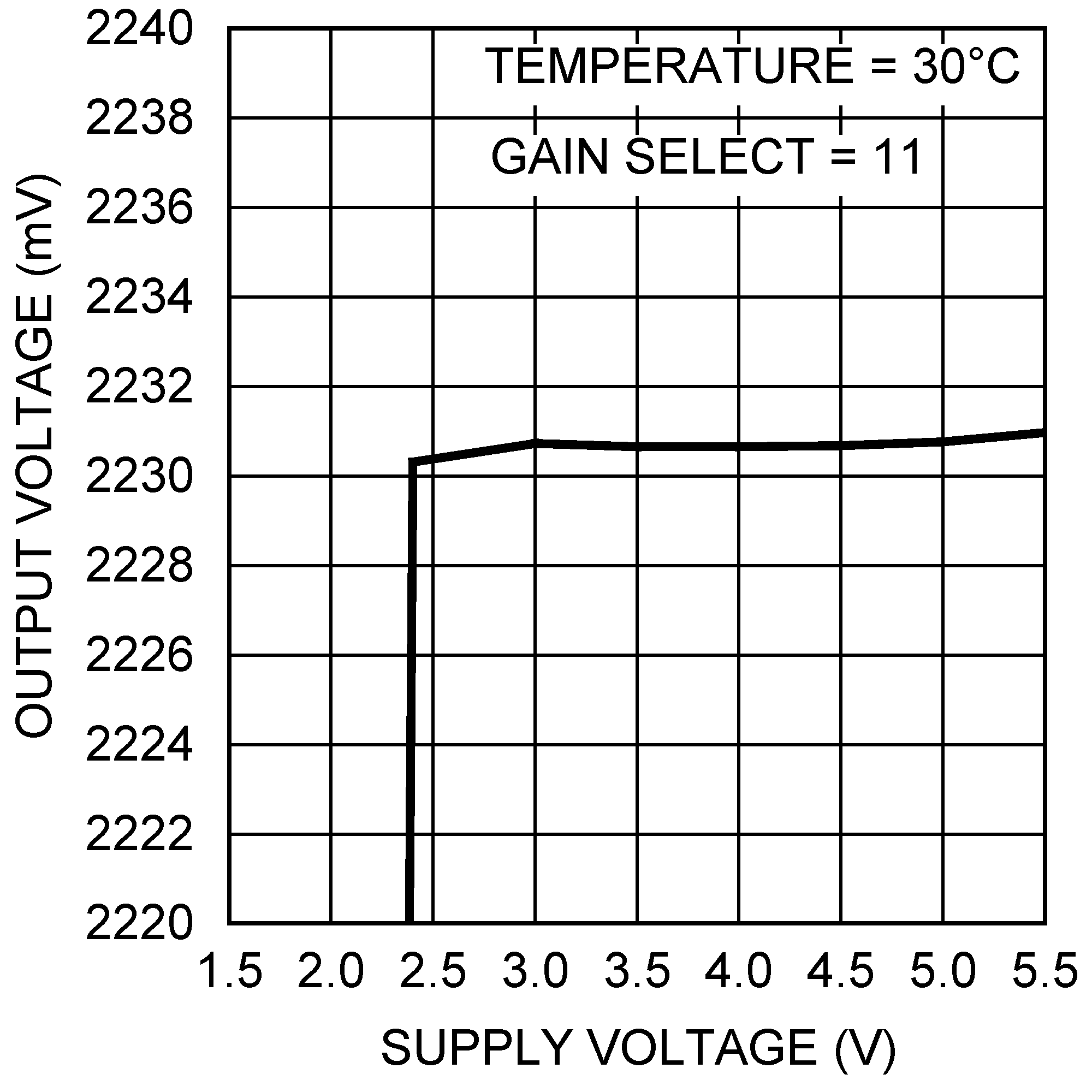 Figure 12. Output Voltage vs. Supply Voltage
 Gain Select = 11