SNOSCY4E March   2015  – October 2018 LMG5200

PRODUCTION DATA.  

  1. Features
  2. Applications
  3. Description
    1.     Device Images
      1.      Simplified Block Diagram
  4. Revision History
  5. Pin Configuration and Functions
    1.     Pin Functions
  6. Specifications
    1. 6.1 Absolute Maximum Ratings
    2. 6.2 ESD Ratings
    3. 6.3 Recommended Operating Conditions
    4. 6.4 Thermal Information
    5. 6.5 Electrical Characteristics
    6. 6.6 Typical Characteristics
  7. Parameter Measurement Information
    1. 7.1 Propagation Delay and Mismatch Measurement
  8. Detailed Description
    1. 8.1 Overview
    2. 8.2 Functional Block Diagram
    3. 8.3 Feature Description
      1. 8.3.1 Control Inputs
      2. 8.3.2 Start-up and UVLO
      3. 8.3.3 Bootstrap Supply Voltage Clamping
      4. 8.3.4 Level Shift
    4. 8.4 Device Functional Modes
  9. Application and Implementation
    1. 9.1 Application Information
    2. 9.2 Typical Application
      1. 9.2.1 Design Requirements
      2. 9.2.2 Detailed Design Procedure
        1. 9.2.2.1 VCC Bypass Capacitor
        2. 9.2.2.2 Bootstrap Capacitor
        3. 9.2.2.3 Power Dissipation
      3. 9.2.3 Application Curves
  10. 10Power Supply Recommendations
  11. 11Layout
    1. 11.1 Layout Guidelines
    2. 11.2 Layout Examples
  12. 12Device and Documentation Support
    1. 12.1 Device Support
      1. 12.1.1 Development Support
    2. 12.2 Documentation Support
      1. 12.2.1 Related Documentation
    3. 12.3 Receiving Notification of Documentation Updates
    4. 12.4 Community Resources
    5. 12.5 Trademarks
    6. 12.6 Electrostatic Discharge Caution
    7. 12.7 Glossary
  13. 13Mechanical, Packaging, and Orderable Information
    1. 13.1 Package Information

Package Options

Mechanical Data (Package|Pins)
Thermal pad, mechanical data (Package|Pins)
Orderable Information

Typical Characteristics

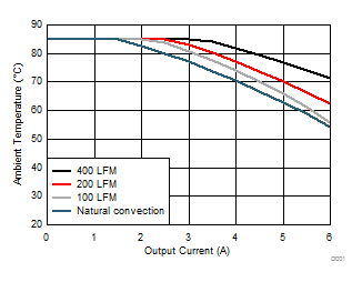
All the curves are based on measurements made on a PCB design with dimensions of 3.2 inches (W) × 2.7 inches (L) × 0.062 inch (T) and 4 layers of 2 oz copper. The safe operating area (SOA) curves displays the temperature boundaries within an operating system by incorporating the thermal resistance and system power loss. A buck converter is used for measuring the SOA. Figure 2 outlines the temperature and airflow conditions required for a given load current. The area under the curve dictates the SOA for different airflow conditions.
LMG5200 D001_SNOSCY4.gif
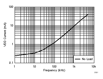
VDD = 5 V
Figure 1. VDD Supply Current vs Switching Frequency
LMG5200 D008_SNOSCY4.gif
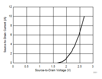
GaN third quadrant conduction.
Figure 3. Source-to-Drain Current vs Source-to-Drain Voltage
LMG5200 D002_SNOSCY4.gif
VIN = 48 V VOUT = 5 V fSW = 1 MHz
Figure 2. Safe Operating Area
LMG5200 D011_SNOSCY4.gif
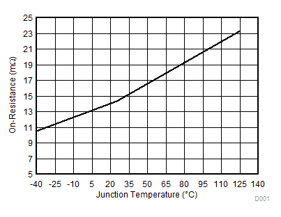
.
Figure 4. GaN FET On-Resistance vs Junction Temperature