SNLS508 September 2015 LMH0318
PRODUCTION DATA.
- 1 Features
- 2 Applications
- 3 Description
- 4 Revision History
- 5 Description continued
- 6 Pin Configuration and Functions
- 7 Specifications
-
8 Detailed Description
- 8.1 Overview
- 8.2 Functional Block Diagram
- 8.3
Feature Description
- 8.3.1 Loss of Signal Detector
- 8.3.2 Continuous Time Linear Equalizer (CTLE)
- 8.3.3 2:1 Multiplexer
- 8.3.4 Clock and Data Recovery
- 8.3.5 Eye Opening Monitor (EOM)
- 8.3.6 Fast EOM
- 8.3.7 LMH0318 Device Configuration
- 8.3.8 Power-On Reset
- 8.4 Device Functional Modes
- 8.5 Programming
- 9 Application and Implementation
- 10Power Supply Recommendations
- 11Layout
- 12Device and Documentation Support
- 13Mechanical, Packaging, and Orderable Information
Package Options
Mechanical Data (Package|Pins)
- RTW|24
Thermal pad, mechanical data (Package|Pins)
- RTW|24
Orderable Information
9 Application and Implementation
NOTE
Information in the following applications sections is not part of the TI component specification, and TI does not warrant its accuracy or completeness. TI’s customers are responsible for determining suitability of components for their purposes. Customers should validate and test their design implementation to confirm system functionality.
9.1 Application Information
The LMH0318 is a single channel SDI reclocker with integrated cable driver that supports different application spaces. The following sections describe the typical use cases and common implementation practices.
9.1.1 General Guidance for All Applications
The LMH0318 supports two modes of configuration: SPI Mode, and SMBus Mode. Once one of these two control mechanism is chosen, pay attention to the PCB layout for the high speed signals. The LMH0318 has strong equalization capabilities that allow it to recover data over lossy channels. As a result, the optimal placement for the LMH0318 is with the higher loss channel at its input and lower loss channel segment at the output in order to meet the various SMPTE requirements. The SMPTE specifications also define the use of AC coupling capacitors for transporting uncompressed serial data streams with heavy low frequency content. This specification requires the use of a 4.7 µF AC coupling capacitor to avoid low frequency DC wander. The 75 Ω signal is also required to meet certain rise/fall timing to facilitate highest eye opening for the receiving device. The LMH0318 built-in 75 Ω termination minimizes parasitic, improving overall signal integrity. Note: When the FPGA is not transmitting valid SMPTE data, the FPGA output should be muted (P=N).
9.2 Typical Application
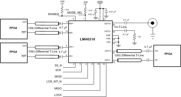
 Figure 17. LMH0318 SPI Mode Configuration
SMPTE specifies the requirements for the Serial Digital Interface to transport digital video at SD, HD, 3Gb/s and higher data rates over coaxial cables. One of the requirements is meeting the required return loss. This requirement specifies how closely the port resembles 75 Ω impedance across a specified frequency band. Output return loss is dependent on board design. The LMH0318 meets this requirement. To gain additional return loss margin, a return loss network, as shown in Figure 18, can be used on the output .
 Figure 18. LMH0318 SPI Mode Configuration with Return Loss Network
9.2.1 Design Requirements
For the LMH0318 design example, the requirements noted in Table 9 apply.
Table 9. LMH0318 Design Parameters
| DESIGN PARAMETER | REQUIREMENT |
|---|---|
| Input AC coupling capacitors | Required. 4.7 µF AC coupling capacitors are recommended. Capacitors may be implemented on the PCB or in the connector. |
| Output AC coupling capacitors | Required. Both OUT0 and OUT1 require AC coupling capacitors. OUT0 AC Coupling capacitors is expected to be 4.7 µF to comply with SMPTE wander requirement. |
| DC Power Supply Coupling Capacitors | To minimize power supply noise, use 0.01 µF capacitors as close to the device VDD pins as possible. |
| Distance from Device to BNC | Keep this distance as short as possible. |
| High Speed IN0, IN1, OUT0, and OUT1 trace impedance | Design differential trace impedance of IN0, IN1, and OUT1 with 100 Ω ± 5%, single-ended trace impedance for OUT0 with 75 Ω ± 5% |
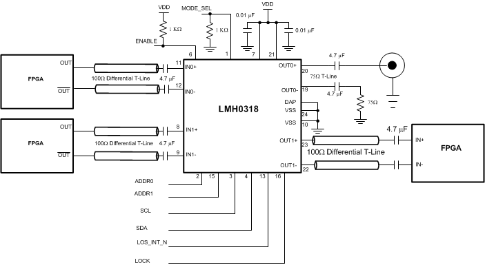
 Figure 19. LMH0318 SMBus Mode Configuration
9.2.2 Detailed Design Procedure
To begin the design process, determine the following:
- Maximum power draw for PCB regulator selection. In this case, use the transient CDR power (during acquisition) specified in the datasheet, multiplied by the number of channels.
- Maximum operational power for thermal calculation. For thermal calculation, use the locked power number. Transient power consumption is only observed during lock acquisition, which typically lasts for <5ms. Additional margin can be applied in case of unsupported data rates being applied which extend the lock time. Note that the CDR should operate in bypass mode for any unsupported data rates.
- Consult the BNC vendor for optimum BNC landing pattern.
- Use IBIS-AMI model for simple channel simulation before PCB layout.
- Closely compare schematic against typical connection diagram in the data sheet.
- Plan out the PCB layout and component placement to minimize parasitic.
9.2.3 Application Curves
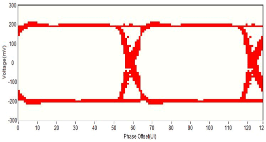
Two common ways to visualize this data are shown in Figure 20 and Figure 21. These diagrams depict examples of eye monitor plot implemented by software. The first plot is an example of using the EOM data to plot a basic eye using ASCII characters, which can be useful for simple diagnostics software. The second plot shows the first derivative of the EOM data, revealing the density of hits and the actual waveforms and crossing that comprise the eye. Measurements were done at default operating conditions.


9.3 Do's and Don'ts
In order to meet SMPTE standard requirements for jitter, AC timing, and return loss use the following guidelines:
- Do place BNC as close to the device as possible.
- Do consult BNC vendor to provide optimum landing pad for the BNC to comply with the required specifications.
- Place return loss network as close to the device as possible.
- Do pay attention to the recommended solder paste to ensure reliable GND connection to DAP.
- Do use control impedance for both 100 Ω and 75 Ω for IN0/1 and OUT0/1.
9.4 Initialization Set Up
After power up or register reset write the initialization sequences in Table 10.
Table 10. LMH0318 Register Initialization
| DESCRIPTION | ADDRESS [Hex] | VALUE [Hex] |
|---|---|---|
| Enable Channel Registers | 0xFF | 0x04 |
| Enable Full Temperature Range | 0x16 | 0x25 |
| Initialize CDR State Machine Control | 0x3E | 0x00 |
| 0x55 | 0x02 | |
| 0x6A | 0x00 | |
| Restore media CTLE setting(1) | 0x03 | xx (2) |
| Reset CDR | 0x0A | 0x5C |
| Release Reset | 0x0A | 0x50 |