SNLS508 September 2015 LMH0318
PRODUCTION DATA.
- 1 Features
- 2 Applications
- 3 Description
- 4 Revision History
- 5 Description continued
- 6 Pin Configuration and Functions
- 7 Specifications
-
8 Detailed Description
- 8.1 Overview
- 8.2 Functional Block Diagram
- 8.3
Feature Description
- 8.3.1 Loss of Signal Detector
- 8.3.2 Continuous Time Linear Equalizer (CTLE)
- 8.3.3 2:1 Multiplexer
- 8.3.4 Clock and Data Recovery
- 8.3.5 Eye Opening Monitor (EOM)
- 8.3.6 Fast EOM
- 8.3.7 LMH0318 Device Configuration
- 8.3.8 Power-On Reset
- 8.4 Device Functional Modes
- 8.5 Programming
- 9 Application and Implementation
- 10Power Supply Recommendations
- 11Layout
- 12Device and Documentation Support
- 13Mechanical, Packaging, and Orderable Information
Package Options
Mechanical Data (Package|Pins)
- RTW|24
Thermal pad, mechanical data (Package|Pins)
- RTW|24
Orderable Information
11 Layout
11.1 Layout Guidelines
The following guidelines should be followed when designing the layout:
- Set trace impedances to 75 Ω ± 5% single ended, 100 Ω ± 5% differential.
- Maintain the same signal reference plane for 75 Ω single-end trace, and reference plane for 100 Ω differential traces.
- Use the smallest size surface mount components.
- Use solid planes. Provide GND or VDD relief under the component pads to minimize parasitic capacitance.
- Select trace widths that minimize the impedance mismatch along the signal path.
- Select a board stack-up that supports 75 Ω or 50 Ω single-end trace, 100 Ω coupled differential traces.
- Use surface mount ceramic capacitors.
- Place return loss network as close to the device as possible.
- Maintain symmetry on the complimentary signals.
- Route 100 Ω traces uniformly (keep trace widths and trace spacing uniform along the trace).
- Avoid sharp bends; use 45-degree or radial bends.
- Walk along the signal path, identify geometry changes and estimate their impedance changes.
- Maintain 75 Ω impedance with a well-designed connectors’ footprint.
- Consult a 3-D simulation tool to guide layout decisions.
- Use the shortest path for VDD and Ground hook-ups; connect pin to planes with vias to minimize or eliminate trace.
- When a high speed trace changes layer, provide at least 2 return vias to improve current return path.
11.2 Layout Example
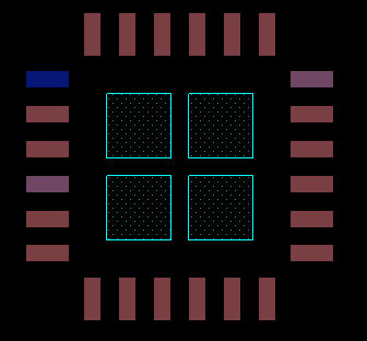
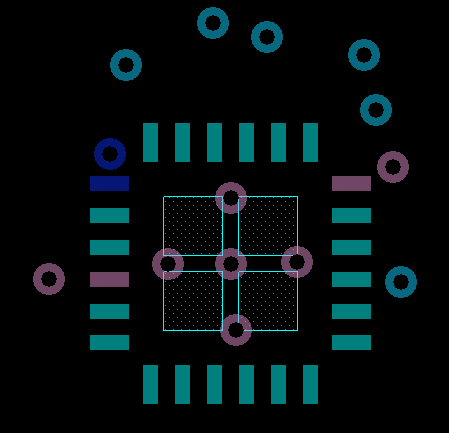
The following example layout demonstrates how the thermal pad should be laid out using standard WQFN board routing guidelines.

Note: Thermal pad is divided into 4 squares with solder paste
Figure 22. LMH0318 Recommended Four Squares Solder Paste

5 Vias without solder paste are located between 4 squares solder paste
Figure 23. LMH0318 Recommended Solder Paste Mask and vias

Top etch plus traces
Figure 24. Example Layout
11.3 Solder Profile
The LMH0318 RTW024A Package solder profile and solder paste material can be found at the following link: SNOA401