SBOS695A August 2014 – December 2014 LMH3401
PRODUCTION DATA.
- 1 Features
- 2 Applications
- 3 Description
- 4 Revision History
- 5 Device Comparison Table
- 6 Pin Configuration and Functions
- 7 Specifications
- 8 Parameter Measurement Information
- 9 Detailed Description
-
10Application and Implementation
- 10.1 Application Information
- 10.2 Typical Application
- 10.3 Do's and Don'ts
- 11Power-Supply Recommendations
- 12Layout
- 13Device and Documentation Support
- 14Mechanical, Packaging, and Orderable Information
Package Options
Mechanical Data (Package|Pins)
- RMS|14
Thermal pad, mechanical data (Package|Pins)
Orderable Information
8 Parameter Measurement Information
8.1 Output Reference Points
The LMH3401 has on-chip output load resistors. When matching the output to a 100-Ω load, the evaluation module (EVM) uses external 40-Ω resistors to complete the output matching. Having on-chip output resistors creates two potential reference points for measuring the output voltage. The amplifier output pins are one output reference point (OUT_AMP). The other output reference point is the point at the matched 100-Ω load (OUT_LOAD). These points are illustrated in Figure 49 to Figure 53; see the Test Schematics section.
Most measurements in the Electrical Characteristics tables and in the Typical Characteristics are measured with reference to the OUT_AMP reference point. The conversion between reference points is a straightforward correction of 3 dB for power and 6 dB for voltage, as shown in Equation 1. The measurements are referenced to OUT_AMP when not specified.
8.2 ATE Testing and DC Measurements
All production testing and ensured dc parameters are measured on automated test equipment capable of dc measurements only. Measurements such as output current sourcing and sinking are made in reference to the device output pins. Some measurements such as voltage gain are referenced to the output of the internal amplifier and do not include losses attributed to the on-chip output resistors. The Electrical Characteristics table conditions specify these conditions. When the measurement is referred to the amplifier output, then the output resistors are not included in the measurement. If the measurement is referred to the device pins, then the output resistor loss is included in the measurement.
8.3 Frequency Response
This test is run with both single-ended inputs and differential inputs.
For tests with single-ended inputs, the standard EVM is used with no changes; see Figure 49. In order to provide a matched input, the unused input requires a broadband 50-Ω termination to be connected. When using a four-port network analyzer, the unused input can either be terminated with a broadband load, or can be connected to the unused input on the four-port analyzer. The network analyzer provides proper termination. A network analyzer is connected to the input and output of the EVM with 50-Ω coaxial cables and is set to measure the forward transfer function (s21). The input signal frequency is swept with the signal level set for the desired output amplitude.
The LMH3401 is fully symmetrical, either input (IN+ or IN–) can be used for single-ended inputs. The unused input must be terminated.
For tests with differential inputs, the same setup for single-ended inputs is used except all four connectors are connected to a network analyzer port. Measurements are made in either true differential mode on the Rohde & Schwarz® network analyzer or in calculated differential mode. In both cases, the differential inputs are each driven with a 50-Ω source. External resistors are recommended if a matched condition is desired because the LMH3401 does not provide an input match for 100-Ω differential sources. Both unterminated (Figure 50) and terminated (Figure 51) differential input measurements are included in this data sheet. The termination is clearly marked in the figure conditions.
8.4 S-Parameters
The standard EVM is used for all s-parameter measurements. All four ports are used or are terminated with
50 Ω, as in the Frequency Response section.
8.5 Frequency Response with Capacitive Load
The standard EVM is used and the capacitive load is soldered to the inside pads of the 40-Ω matching resistors (on the DUT side). This this configuration, the on-chip, 10-Ω resistors isolate the capacitive load from the amplifier output pins. The test schematic for capacitive load measurements is illustrated in Figure 52.
8.6 Distortion
The standard EVM is used for measuring single-tone harmonic distortion and two-tone intermodulation distortion. All distortion is measured with single-ended input signals; see Figure 53. In order to interface with single-ended test equipment, external baluns are required between the EVM output ports and the test equipment. The Typical Characteristics plots were created using Marki™ baluns, model number BAL-0010. These baluns are used to combine two tones in the two-tone tests. For distortion measurements the same termination must be used on both input pins. When a filter is used on the driven input port, the same filter and a broadband load is used to terminate the other input. When the signal source is a broadband controlled impedance, then only a broadband controlled impedance is required to terminate the unused input.
8.7 Noise Figure
The standard EVM is used with a single-ended input and the Marki balun on the output. The noise figure is based on an active input match provided by the on-chip resistor network.
8.8 Pulse Response, Slew Rate, Overdrive Recovery
The standard EVM is used for time-domain measurements. The input is single-ended while the differential outputs are routed directly to the oscilloscope inputs. The differential signal response is calculated from the two separate oscilloscope inputs. In addition, the common-mode response is also captured in this configuration.
8.9 Power Down
The standard EVM is used with the shorting block on jumper JPD removed completely. A high-speed, 50-Ω pulse generator is used to drive the PD pin while the output signal is measured by viewing the output signal (such as a 250-MHz sine wave).
8.10 VCM Frequency Response
The standard EVM is used with Rcm+ and Rcm– removed and a new resistor installed at Rtcm = 49.9 Ω; C17. A network analyzer is connected to the VCM input of the EVM and the EVM outputs are connected to the network analyzer with 50-Ω coaxial cables. Set the network analyzer analysis settings to single-ended input and differential output. Measure the output common-mode with respect to the single-ended input (Scs21). The input signal frequency is swept with the signal level set for 100 mV (–16 dBm). Note that the common-mode control circuit gain is one.
8.11 Test Schematics
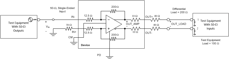 Figure 49. Test Schematic: Single-Ended Input, Differential Output
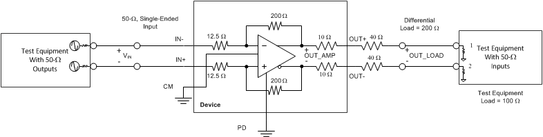 Figure 50. Test Schematic: Differential Input, No Input Match
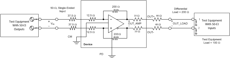 Figure 51. Test Schematic: Differential Input, Input Matched to 100-Ω Differential
Note that in Figure 50, even though the amplifier gain is AV = 200 / 12.5 = 16 V/V (or 24 dB) there is a significant loss at the input resulting from the low input impedance. With 50-Ω test equipment this loss is 12.5 / (50 + 12.5) = 0.2 V/V (or –10 dB). The loss created by the low input impedance puts the net gain for this circuit at 14 dB, only slightly higher than the gain for the fully-terminated configuration of 12 dB. In most applications the external input termination resistors are worth the cost.
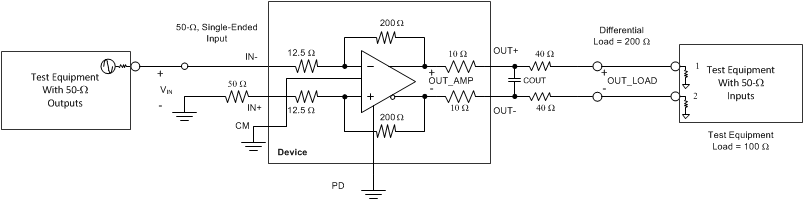 Figure 52. Test Schematic for Capacitive Load
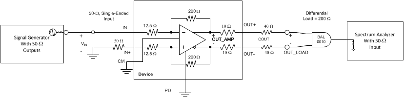 Figure 53. Test Schematic for Harmonic Distortion