SBOS695A August 2014 – December 2014 LMH3401
PRODUCTION DATA.
- 1 Features
- 2 Applications
- 3 Description
- 4 Revision History
- 5 Device Comparison Table
- 6 Pin Configuration and Functions
- 7 Specifications
- 8 Parameter Measurement Information
- 9 Detailed Description
-
10Application and Implementation
- 10.1 Application Information
- 10.2 Typical Application
- 10.3 Do's and Don'ts
- 11Power-Supply Recommendations
- 12Layout
- 13Device and Documentation Support
- 14Mechanical, Packaging, and Orderable Information
Package Options
Mechanical Data (Package|Pins)
- RMS|14
Thermal pad, mechanical data (Package|Pins)
Orderable Information
7 Specifications
7.1 Absolute Maximum Ratings
over operating free-air temperature range (unless otherwise noted)(1)| MIN | MAX | UNIT | ||
|---|---|---|---|---|
| Voltage | Power supply | 5.5 | V | |
| Input voltage range | VS– – 0.7 | VS+ + 0.7 | V | |
| Current | Input current, IN+, IN– | 10 | mA | |
| Output current (sourcing or sinking) OUT+, OUT– | 100 | mA | ||
| Continuous power dissipation | See Thermal Information | |||
| Temperature | Maximum junction temperature, TJ | 150 | °C | |
| Maximum junction temperature, continuous operation, long-term reliability | 125 | °C | ||
| Operating free-air, TA | –40 | 85 | °C | |
| Storage, Tstg | –40 | 150 | °C | |
(1) Stresses beyond those listed under Absolute Maximum Ratings may cause permanent damage to the device. These are stress ratings only, which do not imply functional operation of the device at these or any other conditions beyond those indicated under Recommended Operating Conditions. Exposure to absolute-maximum-rated conditions for extended periods may affect device reliability.
7.2 ESD Ratings
| VALUE | UNIT | |||
|---|---|---|---|---|
| V(ESD) | Electrostatic discharge | Human body model (HBM), per ANSI/ESDA/JEDEC JS-001(1) | ±2500 | V |
| Charged device model (CDM), per JEDEC specification JESD22-C101(2) | ±1000 | |||
(1) JEDEC document JEP155 states that 500-V HBM allows safe manufacturing with a standard ESD control process.
(2) JEDEC document JEP157 states that 250-V CDM allows safe manufacturing with a standard ESD control process.
7.3 Recommended Operating Conditions
over operating free-air temperature range (unless otherwise noted)| MIN | NOM | MAX | UNIT | ||
|---|---|---|---|---|---|
| Supply voltage (VS = VS+ – VS–) | 3.15 | 5 | 5.25 | V | |
| Operating junction temperature, TJ | –40 | 125 | °C | ||
| Ambient operating air temperature, TA | –40 | 25 | 85 | °C | |
7.4 Thermal Information
| THERMAL METRIC(1) | LMH3401 | UNIT | |
|---|---|---|---|
| RMS (UQFN) | |||
| 14 PINS | |||
| RθJA | Junction-to-ambient thermal resistance | 101 | °C/W |
| RθJC(top) | Junction-to-case (top) thermal resistance | 51 | |
| RθJB | Junction-to-board thermal resistance | 61 | |
| ψJT | Junction-to-top characterization parameter | 4.2 | |
| ψJB | Junction-to-board characterization parameter | 61 | |
| RθJC(bot) | Junction-to-case (bottom) thermal resistance | N/A | |
(1) For more information about traditional and new thermal metrics, see the IC Package Thermal Metrics application report, SPRA953.
7.5 Electrical Characteristics: VS = 5 V
Test conditions are at TA = 25°C, VS+ = 2.5 V, VS– = –2.5 V, VCM = 0 V, RL = 200-Ω differential, G = 16 dB, single-ended input and differential output, and input and output referenced to midsupply, unless otherwise noted. Measured using an evaluation module (EVM) as discussed in the Parameter Measurement Information section.| PARAMETER | TEST CONDITIONS | MIN | TYP | MAX | UNIT | TEST LEVEL(1) |
||
|---|---|---|---|---|---|---|---|---|
| AC PERFORMANCE | ||||||||
| Small-signal bandwidth | VO = 200 mVPP(3) | 7 | GHz | C | ||||
| Large-signal bandwidth | VO = 2 VPP | 4 | GHz | C | ||||
| Bandwidth for 0.1-dB flatness | VO = 2 VPP | 700 | MHz | C | ||||
| Slew rate | VO = 2-V step | 18000 | V/µs | C | ||||
| Rise time | VO = 1-V step | 80 | ps | C | ||||
| Fall time | VO = 1-V step | 80 | ps | C | ||||
| Settling time to 1% | VO = 2-V step | 1 | ns | C | ||||
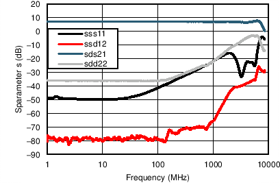
| Input return loss, s11 | See S-Parameters section, f < 1 GHz | –20 | dB | C | ||||
| Output return loss, s22 | See S-Parameters section, f < 1 GHz | –20 | dB | C | ||||
| Reverse isolation, s12 | See S-Parameters section, f < 1 GHz | –65 | dB | C | ||||
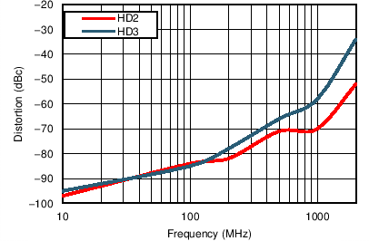
| Second-order harmonic distortion | f = 10 MHz, VO = 2 VPP | –96 | dBc | C | ||||
| f = 500 MHz, VO = 2 VPP | –79 | dBc | C | |||||
| f = 1 GHz, VO = 2 VPP | –64 | dBc | C | |||||
| f = 2 GHz, VO = 2 VPP | –55 | dBc | C | |||||
| Third-order harmonic distortion | f = 10 MHz, VO = 2 VPP | –102 | dBc | C | ||||
| f = 500 MHz, VO = 2 VPP | –77 | dBc | C | |||||
| f = 1 GHz, VO = 2 VPP | –72 | dBc | C | |||||
| f = 2 GHz, VO = 2 VPP | –40 | dBc | C | |||||
| Second-order intermodulation distortion | f = 10 MHz, VO = 1 VPP per tone | –90 | dBc | C | ||||
| f = 500 MHz, VO = 1 VPP per tone | –77 | dBc | C | |||||
| f = 1 GHz, VO = 1 VPP per tone | –71 | dBc | C | |||||
| f = 2 GHz, VO = 1 VPP per tone | –56 | dBc | C | |||||
| Third-order intermodulation distortion | f = 10 MHz, VO = 1 VPP per tone | –101 | dBc | C | ||||
| f = 500 MHz, VO = 1 VPP per tone | –86 | dBc | C | |||||
| f = 1 GHz, VO = 1 VPP per tone | –73 | dBc | C | |||||
| f = 2 GHz, VO = 1 VPP per tone | –52 | dBc | C | |||||
| 1-dB compression point | f = 200 MHz, power measured at amplifier | 13 | dBm | C | ||||
| Output third-order intercept point | At device outputs, f = 200 MHz | 45 | dBm | C | ||||
| At device outputs, f = 1000 MHz | 33 | dBm | C | |||||
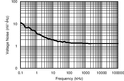
| Input-referred voltage noise | f > 1 MHz | 1.4 | nV/√Hz | C | ||||
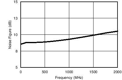
| Noise figure | 50-Ω, single-ended source | f = 200 MHz | 9 | dB | C | |||
| f = 1 GHz | 9.4 | dB | C | |||||
| Overdrive recovery | Overdrive = ±0.5 V | 300 | ps | C | ||||
| Output balance error | f = 1000 MHz | 45 | dBc | C | ||||
| Output impedance | At dc | 16 | 20 | 24 | Ω | A | ||
| DC PERFORMANCE | ||||||||
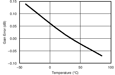
| Gain | 50-Ω single-ended source, with external 50-Ω termination | 15.4 | 16 | 16.6 | dB | A | ||
| 100-Ω differential source, external termination | 12 | dB | C | |||||
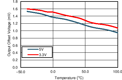
| Differential output offset | TA = 25°C | ±2 | ±20 | mV | A | |||
| TA = –40°C to 85°C | ±4 | mV | C | |||||
| Differential output offset temperature drift | 4 | µV/°C | C | |||||
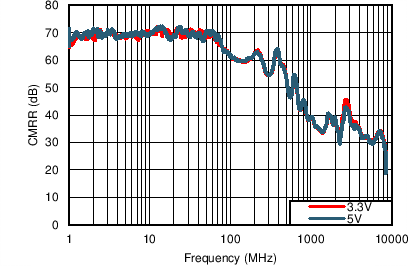
| Common-mode rejection ratio | TA = 25°C | 72 | dBc | C | ||||
| INPUT | ||||||||
| Differential input resistance | 22 | 25 | 29 | Ω | A | |||
| Single ended input resistance | With external 50-Ω resistor on INN to ground | 45 | 50 | 55 | Ω | A | ||
| Input common-mode range low | Inputs shorted together, VCM = 2.5 V | VS– – 0.7 | VS– + 0.2 | V | A | |||
| Input common-mode range high | Inputs shorted together, VCM = 2.5 V | VS+ – 1.3 | VS+ – 1.2 | V | A | |||
| OUTPUT | ||||||||
| Output voltage range high | Measured single-ended | TA = 25°C | VS+ – 1.3 | VS+ – 1.1 | V | A | ||
| TA = –40°C to 85°C | VS+ – 1.2 | V | C | |||||
| Output voltage range low | Measured single-ended | TA = 25°C | VS– + 1.3 | VS– + 1.1 | V | A | ||
| TA = –40°C to 85°C | VS– + 1.2 | V | C | |||||
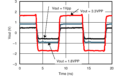
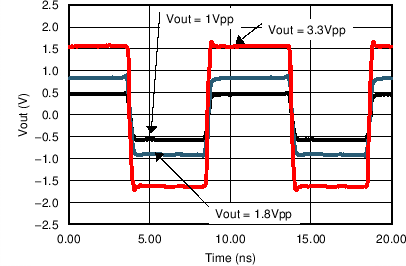
| Differential output voltage | 5.6 | VPP | C | |||||
| Differential output current drive | VO = 0 V | 40 | 50 | mA | A | |||
| OUTPUT COMMON-MODE VOLTAGE CONTROL | ||||||||
| VCM small-signal bandwidth | VOUT_CM = 200 mVPP | 3.3 | GHz | C | ||||
| VCM slew rate | VOUT_CM = 500 mVPP | 2900 | V/µs | C | ||||
| VCM voltage range low | Differential gain shift < 1 dB | VS– + 1.6 | VS– + 2.0 | V | A | |||
| VCM voltage range high | Differential gain shift < 1 dB | VS+ – 2.0 | VS+ – 1.6 | V | A | |||
| VCM gain | VCM = 0 V | 0.98 | 1.0 | 1.01 | V/V | A | ||
| VOUT_CM output common-mode offset from VCM input voltage (2) |
VCM = 0 V | –27 | mV | C | ||||
| VCM temperature drift | –13.6 | µV/°C | C | |||||
| POWER SUPPLY | ||||||||
| Quiescent current | TA = 25°C | 50 | 55 | 62 | mA | A | ||
| Power-supply rejection ratio | VS+ | 60 | 84 | dB | A | |||
| VS– | 50 | 75 | dB | A | ||||
| POWER DOWN | ||||||||
| Enable or disable voltage threshold | Device powers on below 0.8 V, device powers down above 1.2 V |
0.9 | 1.1 | 1.2 | V | A | ||
| Power-down quiescent current | 1 | 3 | 6 | mA | A | |||
| PD bias current | PD = 2.5 V | 10 | ±100 | µA | C | |||
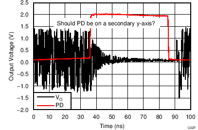
| Turn-on time delay | Time to VO = 90% of final value | 10 | ns | C | ||||
| Turn-off time delay | Time to VO = 10% of original value | 10 | ns | C | ||||
(1) Test levels: (A) 100% tested at 25°C. Overtemperature limits by characterization and simulation. (B) Limits set by characterization and simulation. (C) Typical value only for information.
(2) VOUT_CM = (OUT+ + OUT–) / 2 and is set by the CM pin VOUT_CM ≈ VCM.
(3) All output voltages are specified as differential voltages unless otherwise noted. Output differential voltage is defined as VO = (VO+ – VO–).
7.6 Electrical Characteristics: VS = 3.3 V
Test conditions are at TA = 25°C, VS+ = 1.65 V, VS– = –1.65 V, VCM = 0 V, RL = 200-Ω differential, G = 16 dB, single-ended input and differential output, and input and output referenced to midsupply, unless otherwise noted. Measured using an EVM as discussed in the Parameter Measurement Information section.| PARAMETER | TEST CONDITIONS | MIN | TYP | MAX | UNIT | TEST LEVEL(1) |
||
|---|---|---|---|---|---|---|---|---|
| AC PERFORMANCE | ||||||||
| Small-signal bandwidth | VO = 200 mVPP | 6.5 | GHz | C | ||||
| Large-signal bandwidth | VO = 1 VPP | 4 | GHz | C | ||||
| Bandwidth for 0.1-dB flatness | VO = 1 VPP | 700 | MHz | C | ||||
| Slew rate | VO = 1-V step | 17600 | V/µs | C | ||||
| Rise time | VO = 1-V step | 90 | ps | C | ||||
| Fall time | VO = 1-V step | 90 | ps | C | ||||
| Input return loss, s11 | See S-Parameters section, f < 1 GHz | –20 | dB | C | ||||
| Output return loss, s22 | See S-Parameters section, f < 1 GHz | –20 | dB | C | ||||
| Reverse isolation, s12 | See S-Parameters section, f < 1 GHz | –65 | dB | C | ||||
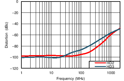
| Second-order harmonic distortion | f = 10 MHz, VO = 1 VPP | –97 | dBc | C | ||||
| f = 500 MHz, VO = 1 VPP | –74 | dBc | C | |||||
| f = 1 GHz, VO = 1 VPP | –59 | dBc | C | |||||
| f = 2 GHz, VO = 1 VPP | –48 | dBc | C | |||||
| Third-order harmonic distortion | f = 10 MHz, VO = 1 VPP | –100 | dBc | C | ||||
| f = 500 MHz, VO = 1 VPP | –66 | dBc | C | |||||
| f = 1 GHz, VO = 1 VPP | –56 | dBc | C | |||||
| f = 2 GHz, VO = 1 VPP | –49 | dBc | C | |||||
| Second-order intermodulation distortion | f = 10 MHz, VO = 0.5 VPP per tone | –95 | dBc | C | ||||
| f = 500 MHz, VO = 0.5 VPP per tone | –81 | dBc | C | |||||
| f = 1 GHz, VO = 0.5 VPP per tone | –72 | dBc | C | |||||
| f = 2 GHz, VO = 0.5 VPP per tone | –60 | dBc | C | |||||
| Third-order intermodulation distortion | f = 10 MHz, VO = 0.5 VPP per tone | –100 | dBc | C | ||||
| f = 500 MHz, VO = 0.5 VPP per tone | –86 | dBc | C | |||||
| f = 1 GHz, VO = 0.5 VPP per tone | –78 | dBc | C | |||||
| f = 2 GHz, VO = 0.5 VPP per tone | –56 | dBc | C | |||||
| Output third-order intercept point | At device outputs, f = 10 MHz | 39.5 | dBm | C | ||||
| At device outputs, f = 1000 MHz | 31 | dBm | C | |||||
| Input-referred voltage noise | f > 1 MHz | 1.4 | nV/√Hz | C | ||||
| Noise figure | 50-Ω, single-ended source | f = 200 MHz | 9 | dB | C | |||
| f = 1 GHz | 9.4 | dB | C | |||||
| Overdrive recovery | Overdrive = ±0.5 V | 400 | ps | C | ||||
| Output impedance | f = 100 MHz | 16 | 20 | 24 | Ω | A | ||
| DC PERFORMANCE | ||||||||
| Gain | 50-Ω, single-ended source with external 50-Ω termination | 15.4 | 16 | 16.6 | dB | A | ||
| 100-Ω differential source, external termination | 12 | dB | C | |||||
| Differential output offset voltage | TA = 25°C | ±2 | ±20 | mV | A | |||
| TA = –40°C to 85°C | ±4 | mV | C | |||||
| Differential output voltage drift | 3.6 | µV/°C | C | |||||
| Common-mode rejection ratio | –72 | dB | A | |||||
| INPUT | ||||||||
| Differential input resistance | 22 | 25 | 29 | Ω | A | |||
| Single-ended input resistance | With external 50-Ω resistor on INN to ground | 45 | 50 | 55 | Ω | A | ||
| Input common-mode range low | Inputs shorted together | VS– – 0.3 | VS– + 0.2 | V | A | |||
| Input common-mode range high | Inputs shorted together | VS+ – 1.5 | VS+ –1.6 | V | A | |||
| OUTPUT | ||||||||
| Output voltage range high | Measured single-ended | TA = 25°C | VS+ – 1.2 | VS+ – 0.95 | V | A | ||
| TA = –40°C to 85°C | VS+ – 1.05 | V | C | |||||
| Output voltage range low | Measured single-ended | TA = 25°C | VS– + 1.2 | VS– + 0.95 | V | A | ||
| TA = –40°C to 85°C | VS– + 1.05 | V | C | |||||
| Differential output voltage | 2.8 | VPP | C | |||||
| Differential output current drive | VO = 0 V | 30 | 40 | mA | A | |||
| OUTPUT COMMON-MODE VOLTAGE CONTROL | ||||||||
| VCM small-signal bandwidth | VOUT_CM = 200 mVPP | 3 | GHz | C | ||||
| VCM slew rate | VOUT_CM = 500 mVPP | 2600 | V/µs | C | ||||
| VCM voltage range low | Differential gain shift < 1 dB | VS– + 1.35 | VS– + 1.55 | V | A | |||
| VCM voltage range high | Differential gain shift < 1 dB | VS+ – 1.55 | VS+ – 1.35 | V | A | |||
| VCM gain | VCM = 0 V | 0.98 | 1.0 | 1.01 | V/V | A | ||
| Output common-mode offset from VCM input |
VCM = 0 V | –7 | mV | C | ||||
| Common-mode voltage drift | –34.6 | µV/°C | C | |||||
| POWER SUPPLY | ||||||||
| Quiescent current | TA = 25°C | 49 | 54 | 60 | mA | A | ||
| Power-supply rejection ratio | VS+ | 60 | 84 | dB | A | |||
| VS– | 50 | 75 | dB | A | ||||
| POWER-DOWN | ||||||||
| Enable or disable voltage threshold | Device powers on below 0.8 V, device powers down above 1.2 V |
1.0 | 1.1 | 1.2 | V | A | ||
| Power-down quiescent current | 1 | 1.6 | 5 | mA | A | |||
| PD bias current | PD = 2.5 V | 10 | ±100 | µA | C | |||
| Turn-on time delay | Time to VO = 90% of final value | 10 | ns | C | ||||
| Turn-off time delay | Time to VO = 10% of original value | 10 | ns | C | ||||
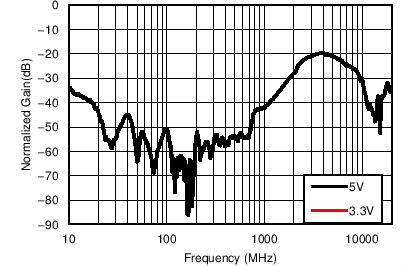
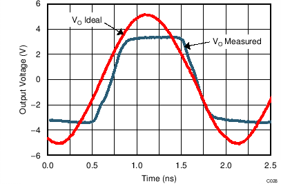
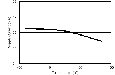
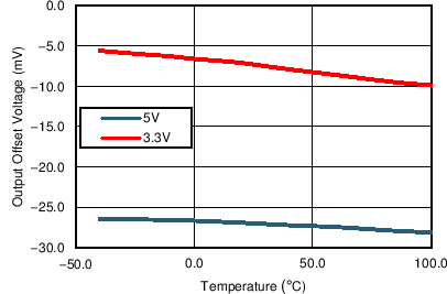
7.7 Typical Characteristics
At TA = 25°C, split supplies, VCM = 0 V, RL = 200-Ω differential (ROUT = 40 Ω each), G = 16 dB, single-ended input and differential output, and input and output pins referenced to midsupply, unless otherwise noted. Measured using an EVM as discussed in the section (see Figure 49 to Figure 53).
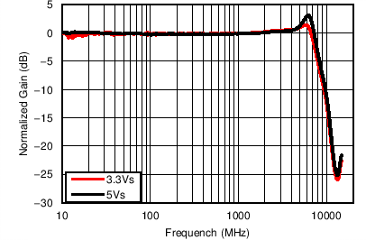
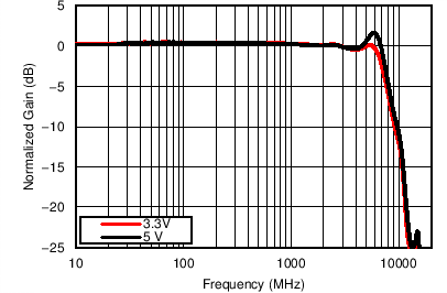
| VS = ±2.5 V, VOUT_AMP = 0.4 VPP | ||
| No input matching resistors, VOUT_AMP = 0.2 VPP, net gain = 14 dB, VS = ±2.5 V |
| VS = ±2.5 V, VOUT_AMP = 4 VPP |
(Single-Ended Input)
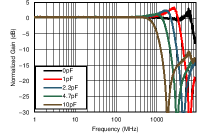
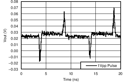
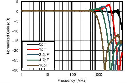
| VS = ±2.5 V, VOUT_AMP = 1 VPP, capacitance at DUT output pins |
| VS = ±2.5 V, VOUT_AMP = 200 mVPP |
| VS = ±2.5 V, VOUT_AMP = 100 mVPP |
| VS = ±2.5 V, VOUT_AMP = 2 VPP |
| VS = ±2.5 V, VOUT_AMP = 2 VPP, f = 1 GHz |
| VS = ±1.65 V, VOUT_AMP = 1 VPP, f = 1 GHz |
| VS = ±1.65 V, f = 200 MHz, VOUT_AMP = 1 VPP |
| VS = ±1.65 V, f = 1000 MHz, VOUT_AMP = 1 VPP |
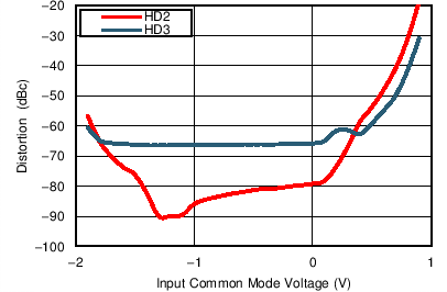
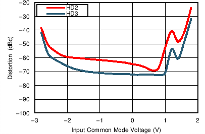
| VS = ±1.65 V, f = 200 MHz, VOUT_AMP = 1 VPP |
| VS = ±1.65 V, f = 500 MHz, VOUT_AMP = 1 VPP |
| VS = ±1.65 V, f = 1 GHz, VOUT_AMP = 1 VPP |
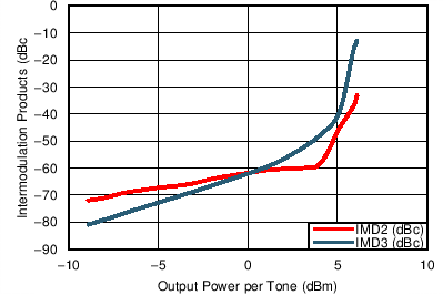
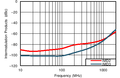
| VS = ±2.5 V, VOUT_AMP = 1 VPP per tone, RLOAD = 100 Ω |
(100-Ω Load)
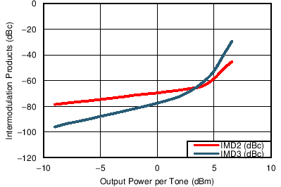
| VS = ±2.5 V, power measured at amplifier |
| VS = ±2.5 V, power measured at amplifier |
| VS = ±2.5 V |
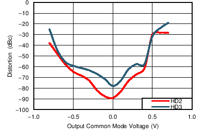
| VS = ±2.5 V, VOUT_AMP, VCM = (VO+ + VO–) / 2 |
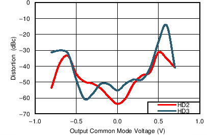
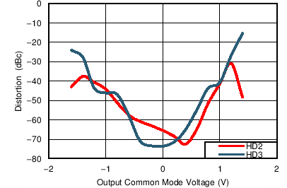
| VS = ±1.65 V, VOUT_AMP |
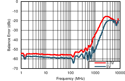
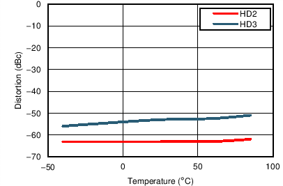
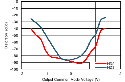
| VS = ±2.5 V |
| VS = ±2.5 V |
| At dc |
| External 37.5-Ω input matching resistors, VOUT_AMP = 0.4 VPP, gain = 12 dB, see Figure 57, VS = ±1.65 V and ±2.5 V |
| Single-ended input, VOUT_AMP = 1 VPP | ||
| VS = ±2.5 V, VOUT_AMP = 1 VPP |
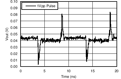
| VS = ±1.65 V, VOUT_AMP = 1 VPP, capacitance at DUT output pins |
| VS = ±1.65 V, VOUT_AMP = 200 mVPP |
| VS = ±1.65 V, VOUT_AMP = 100 mVPP |
| VS = ±2.5 V, VOUT_AMP = 2 VPP, RLOAD = 100 Ω |
| VS = ±1.65 V, VOUT_AMP = 1 VPP |
| VS = ±2.5 V, f = 200 MHz, VOUT_AMP = 2 VPP |
| VS = ±2.5 V, f = 1000 MHz, VOUT_AMP = 2 VPP |
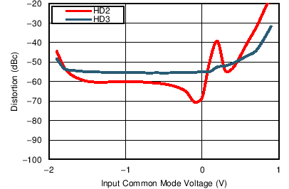
| VS = ±2.5 V, f = 200 MHz, VOUT_AMP = 2 VPP |
| VS = ±2.5 V, f = 500 MHz, VOUT_AMP = 2 VPP |
| VS = ±2.5 V, f = 1 GHz, VOUT_AMP = 2 VPP |
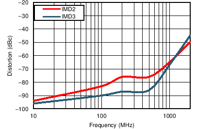
| VS = ±2.5 V, VOUT_AMP = 1 VPP per tone, |
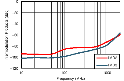
| VS = ±1.65 V, VOUT_AMP = 0.5 VPP per tone |
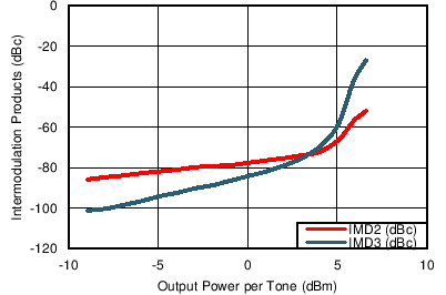
| VS = ±2.5 V, power measured at amplifier |
| VS = ±2.5 V |
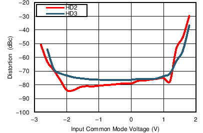
| VS = ±2.5 V, VOUT_AMP |
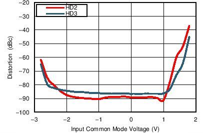
| VS = ±1.65 V, VOUT_AMP |
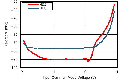
| Differential input |
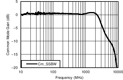
| Common-mode input, common-mode output, RS = 25 Ω, RL = 50 Ω |
| VS = ±2.5 V |
| VS = ±2.5 V |
| At dc |