SBOS710D October   2014  – February 2018 LMH5401

PRODUCTION DATA.  

  1. Features
  2. Applications
    1.     Distortion versus Frequency (G = 12 dB, SE-DE, RL = 200 Ω, VPP = 2 V)
  3. Description
    1.     LMH5401 Driving an ADC12J4000
  4. Revision History
  5. Pin Configuration and Functions
    1.     Pin Functions
  6. Specifications
    1. 6.1 Absolute Maximum Ratings
    2. 6.2 ESD Ratings
    3. 6.3 Recommended Operating Conditions
    4. 6.4 Thermal Information
    5. 6.5 Electrical Characteristics: VS = 5 V
    6. 6.6 Electrical Characteristics: VS = 3.3 V
    7. 6.7 Typical Characteristics: 5 V
    8. 6.8 Typical Characteristics: 3.3 V
    9. 6.9 Typical Characteristics: 3.3-V to 5-V Supply Range
  7. Parameter Measurement Information
    1. 7.1  Output Reference Points
    2. 7.2  ATE Testing and DC Measurements
    3. 7.3  Frequency Response
    4. 7.4  S-Parameters
    5. 7.5  Frequency Response with Capacitive Load
    6. 7.6  Distortion
    7. 7.7  Noise Figure
    8. 7.8  Pulse Response, Slew Rate, and Overdrive Recovery
    9. 7.9  Power Down
    10. 7.10 VCM Frequency Response
    11. 7.11 Test Schematics
  8. Detailed Description
    1. 8.1 Overview
    2. 8.2 Functional Block Diagram
    3. 8.3 Feature Description
      1. 8.3.1 Fully-Differential Amplifier
        1. 8.3.1.1 Power Down and Ground Pins
      2. 8.3.2 Operations for Single-Ended to Differential Signals
        1. 8.3.2.1 AC-Coupled Signal Path Considerations for Single-Ended Input to Differential Output Conversion
        2. 8.3.2.2 DC-Coupled Input Signal Path Considerations for SE-DE Conversions
        3. 8.3.2.3 Resistor Design Equations for Single-to-Differential Applications
        4. 8.3.2.4 Input Impedance Calculations
      3. 8.3.3 Differential-to-Differential Signals
        1. 8.3.3.1 AC-Coupled, Differential-Input to Differential-Output Design Issues
        2. 8.3.3.2 DC-Coupled, Differential-Input to Differential-Output Design Issues
      4. 8.3.4 Output Common-Mode Voltage
      5. 8.3.5 LMH5401 Comparison
    4. 8.4 Device Functional Modes
      1. 8.4.1 Operation With a Split Supply
      2. 8.4.2 Operation With a Single Supply
  9. Application and Implementation
    1. 9.1 Application Information
      1. 9.1.1 Stability
      2. 9.1.2 Input and Output Headroom Considerations
      3. 9.1.3 Noise Analysis
      4. 9.1.4 Noise Figure
      5. 9.1.5 Thermal Considerations
    2. 9.2 Typical Application
      1. 9.2.1 Design Requirements
      2. 9.2.2 Detailed Design Procedure
        1. 9.2.2.1 Driving Matched Loads
        2. 9.2.2.2 Driving Unmatched Loads For Lower Loss
        3. 9.2.2.3 Driving Capacitive Loads
        4. 9.2.2.4 Driving ADCs
          1. 9.2.2.4.1 SNR Considerations
          2. 9.2.2.4.2 SFDR Considerations
          3. 9.2.2.4.3 ADC Input Common-Mode Voltage Considerations : AC-Coupled Input
          4. 9.2.2.4.4 ADC Input Common-Mode Voltage Considerations : DC-Coupled Input
        5. 9.2.2.5 GSPS ADC Driver
        6. 9.2.2.6 Common-Mode Voltage Correction
        7. 9.2.2.7 Active Balun
      3. 9.2.3 Application Curves
    3. 9.3 Do's and Don'ts
      1. 9.3.1 Do:
      2. 9.3.2 Don't:
  10. 10Power Supply Recommendations
    1. 10.1 Supply Voltage
    2. 10.2 Single-Supply
    3. 10.3 Split-Supply
    4. 10.4 Supply Decoupling
  11. 11Layout
    1. 11.1 Layout Guidelines
    2. 11.2 Layout Example
  12. 12Device and Documentation Support
    1. 12.1 Device Support
      1. 12.1.1 Device Nomenclature
    2. 12.2 Documentation Support
      1. 12.2.1 Related Documentation
    3. 12.3 Receiving Notification of Documentation Updates
    4. 12.4 Community Resources
    5. 12.5 Trademarks
    6. 12.6 Electrostatic Discharge Caution
    7. 12.7 Glossary
  13. 13Mechanical, Packaging, and Orderable Information

Package Options

Mechanical Data (Package|Pins)
Thermal pad, mechanical data (Package|Pins)
Orderable Information

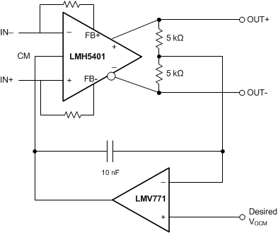
Common-Mode Voltage Correction

The LMH5401 can set the output common-mode voltage to within a typical value of ±30 mV. If greater accuracy is desired, a simple circuit can improve this accuracy by an order of magnitude. A precision, low-power operational amplifier is used to sense the error in the output common-mode of the LMH5401 and corrects the error by adjusting the voltage at the CM pin. In Figure 72, the precision of the op amp replaces the less accurate precision of the LMH5401 common-mode control circuit while still using the LMH5401 common-mode control circuit speed. The op amp in this circuit must have better than a 1-mV input-referred offset voltage and low noise. Otherwise the specifications are not very critical because the LMH5401 is responsible for the entire differential signal path.
LMH5401 ai_cmservo_bos710.gifFigure 72. Common-Mode Correction Circuit