SBOS710D October   2014  – February 2018 LMH5401

PRODUCTION DATA.  

  1. Features
  2. Applications
    1.     Distortion versus Frequency (G = 12 dB, SE-DE, RL = 200 Ω, VPP = 2 V)
  3. Description
    1.     LMH5401 Driving an ADC12J4000
  4. Revision History
  5. Pin Configuration and Functions
    1.     Pin Functions
  6. Specifications
    1. 6.1 Absolute Maximum Ratings
    2. 6.2 ESD Ratings
    3. 6.3 Recommended Operating Conditions
    4. 6.4 Thermal Information
    5. 6.5 Electrical Characteristics: VS = 5 V
    6. 6.6 Electrical Characteristics: VS = 3.3 V
    7. 6.7 Typical Characteristics: 5 V
    8. 6.8 Typical Characteristics: 3.3 V
    9. 6.9 Typical Characteristics: 3.3-V to 5-V Supply Range
  7. Parameter Measurement Information
    1. 7.1  Output Reference Points
    2. 7.2  ATE Testing and DC Measurements
    3. 7.3  Frequency Response
    4. 7.4  S-Parameters
    5. 7.5  Frequency Response with Capacitive Load
    6. 7.6  Distortion
    7. 7.7  Noise Figure
    8. 7.8  Pulse Response, Slew Rate, and Overdrive Recovery
    9. 7.9  Power Down
    10. 7.10 VCM Frequency Response
    11. 7.11 Test Schematics
  8. Detailed Description
    1. 8.1 Overview
    2. 8.2 Functional Block Diagram
    3. 8.3 Feature Description
      1. 8.3.1 Fully-Differential Amplifier
        1. 8.3.1.1 Power Down and Ground Pins
      2. 8.3.2 Operations for Single-Ended to Differential Signals
        1. 8.3.2.1 AC-Coupled Signal Path Considerations for Single-Ended Input to Differential Output Conversion
        2. 8.3.2.2 DC-Coupled Input Signal Path Considerations for SE-DE Conversions
        3. 8.3.2.3 Resistor Design Equations for Single-to-Differential Applications
        4. 8.3.2.4 Input Impedance Calculations
      3. 8.3.3 Differential-to-Differential Signals
        1. 8.3.3.1 AC-Coupled, Differential-Input to Differential-Output Design Issues
        2. 8.3.3.2 DC-Coupled, Differential-Input to Differential-Output Design Issues
      4. 8.3.4 Output Common-Mode Voltage
      5. 8.3.5 LMH5401 Comparison
    4. 8.4 Device Functional Modes
      1. 8.4.1 Operation With a Split Supply
      2. 8.4.2 Operation With a Single Supply
  9. Application and Implementation
    1. 9.1 Application Information
      1. 9.1.1 Stability
      2. 9.1.2 Input and Output Headroom Considerations
      3. 9.1.3 Noise Analysis
      4. 9.1.4 Noise Figure
      5. 9.1.5 Thermal Considerations
    2. 9.2 Typical Application
      1. 9.2.1 Design Requirements
      2. 9.2.2 Detailed Design Procedure
        1. 9.2.2.1 Driving Matched Loads
        2. 9.2.2.2 Driving Unmatched Loads For Lower Loss
        3. 9.2.2.3 Driving Capacitive Loads
        4. 9.2.2.4 Driving ADCs
          1. 9.2.2.4.1 SNR Considerations
          2. 9.2.2.4.2 SFDR Considerations
          3. 9.2.2.4.3 ADC Input Common-Mode Voltage Considerations : AC-Coupled Input
          4. 9.2.2.4.4 ADC Input Common-Mode Voltage Considerations : DC-Coupled Input
        5. 9.2.2.5 GSPS ADC Driver
        6. 9.2.2.6 Common-Mode Voltage Correction
        7. 9.2.2.7 Active Balun
      3. 9.2.3 Application Curves
    3. 9.3 Do's and Don'ts
      1. 9.3.1 Do:
      2. 9.3.2 Don't:
  10. 10Power Supply Recommendations
    1. 10.1 Supply Voltage
    2. 10.2 Single-Supply
    3. 10.3 Split-Supply
    4. 10.4 Supply Decoupling
  11. 11Layout
    1. 11.1 Layout Guidelines
    2. 11.2 Layout Example
  12. 12Device and Documentation Support
    1. 12.1 Device Support
      1. 12.1.1 Device Nomenclature
    2. 12.2 Documentation Support
      1. 12.2.1 Related Documentation
    3. 12.3 Receiving Notification of Documentation Updates
    4. 12.4 Community Resources
    5. 12.5 Trademarks
    6. 12.6 Electrostatic Discharge Caution
    7. 12.7 Glossary
  13. 13Mechanical, Packaging, and Orderable Information

Package Options

Mechanical Data (Package|Pins)
Thermal pad, mechanical data (Package|Pins)
Orderable Information

Noise Analysis

The first step in the output noise analysis is to reduce the application circuit to the simplest form with equal feedback and gain setting elements to ground (as shown in Figure 64) and considering FAD and resistor noise terms.
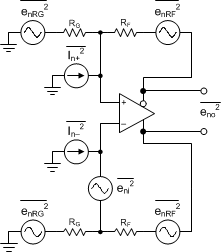
LMH5401 fda_noise_bos695.gifFigure 64. FDA Noise-Analysis Circuit

Figure 64 shows the noise powers for each term. When the RF and RG terms are matched on each side, the total differential output noise is the root sum of squares (RSS) of these separate terms. Using NG (noise gain) ≡ 1 + RF / RG, the total output noise is shown in Equation 8. Each resistor noise term is a 4-kTR power.

Equation 8. LMH5401 q_eo_bos695.gif

The first term is the differential input spot noise times the noise gain. The second term is the input current noise terms times the feedback resistor (and because there are two terms, the power is two times one of the terms). The last term is the output noise resulting from the RF and RG resistors (again times two) for the output noise power of each side added together. Using the exact values for a 50-Ω, matched, single-ended to differential gain, sweep with 127 Ω (plus an internal 25 Ω) and the intrinsic noise eni = 1.25 nV and in = 3.5 pA for the LMH5401, which gives an output spot noise from Equation 8. Then, dividing by the signal gain set through internal resistors (AV), gives the input-referred, spot-noise voltage (ei) of 1.35 nV/√Hz. Note that for the LMH5401 the current noise is an insignificant noise contributor because of the low value of RF.