SBOS710D October 2014 – February 2018 LMH5401
PRODUCTION DATA.
- 1 Features
- 2 Applications
- 3 Description
- 4 Revision History
- 5 Pin Configuration and Functions
-
6 Specifications
- 6.1 Absolute Maximum Ratings
- 6.2 ESD Ratings
- 6.3 Recommended Operating Conditions
- 6.4 Thermal Information
- 6.5 Electrical Characteristics: VS = 5 V
- 6.6 Electrical Characteristics: VS = 3.3 V
- 6.7 Typical Characteristics: 5 V
- 6.8 Typical Characteristics: 3.3 V
- 6.9 Typical Characteristics: 3.3-V to 5-V Supply Range
- 7 Parameter Measurement Information
- 8 Detailed Description
-
9 Application and Implementation
- 9.1 Application Information
- 9.2 Typical Application
- 9.3 Do's and Don'ts
- 10Power Supply Recommendations
- 11Layout
- 12Device and Documentation Support
- 13Mechanical, Packaging, and Orderable Information
Package Options
Mechanical Data (Package|Pins)
- RMS|14
Thermal pad, mechanical data (Package|Pins)
Orderable Information
8.3.2.3 Resistor Design Equations for Single-to-Differential Applications
Being familiar with the FDA resistor selection criteria is still important because the LMH5401 gain is configured through external resistors. The design equations for setting the resistors around an FDA to convert from a single-ended input signal to a differential output can be approached in several ways. In this section, several critical assumptions are made to simplify the results:
- The feedback resistors are selected first and are set to be equal on the two sides of the device.
- The DC and AC impedances from the summing junctions back to the signal source and ground (or a bias voltage on the non-signal input side) are set equal to retain the feedback divider balance on each side of the FDA.
Both of these assumptions are typical and are aimed to deliver the best dynamic range through the FDA signal path.
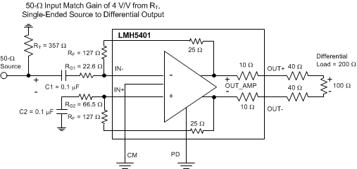
After the feedback resistor values are selected, the aim is to solve for RT (a termination resistor to ground on the signal input side), RG1 (the input gain resistor for the signal path), and RG2 (the matching gain resistor on the non-signal input side); see Figure 61. This example uses the LMH5401, which is an external resistor FDA. The same resistor solutions can be applied to AC- or DC-coupled paths. Adding blocking capacitors in the input-signal chain is a simple option. Adding these blocking capacitors after the RT element (see Figure 61) has the advantage of removing any DC currents in the feedback path from the output VOCM to ground.
 Figure 61. AC-Coupled, Single-Ended Source to a Differential Gain of a 4-V/V
Most FDA amplifiers use external resistors and have complete flexibility in the selected RF. However, the LMH5401 has small on-chip feedback resistors that are fixed at 25 Ω. The equations used in this section apply with an additional 25 Ω to add to the external RF resistors.
After the feedback resistor values are selected, solve for RT (a termination resistor to ground on the signal input side), RG1 (the input gain resistor for the signal path), and RG2 (the matching gain resistor on the non-signal input side). The same resistor solutions are applied to AC- or DC-coupled paths. Adding blocking capacitors in the input-signal chain is a simple option. Adding these blocking capacitors after the RT element has the advantage of removing any DC currents in the feedback path from the output VOCM to ground.
Earlier approaches to the solutions for RT and RG1 (when the input must be matched to a source impedance, RS) follow an iterative approach. This complexity arises from the active input impedance at the RG1 input. When the FDA converts a single-ended signal to a differential signal, the common-mode input voltage at the FDA inputs must move with the input signal to generate the inverted output signal as a current in the RG2 element. A more recent solution is shown as Equation 3, where a quadratic in RT is solved for an exact required value. This quadratic emerges from the simultaneous solution for a matched input impedance and target gain. The only required inputs are:
- The selected RF value.
- The target voltage gain (AV) from the input of RT to the differential output voltage.
- The desired input impedance at the junction of RT and RG1 to match RS.
Solving this quadratic for RT starts the solution sequence, as shown in Equation 3:

Because this equation is a quadratic, there are limits to the range of solutions. Specifically, after RF and RS are selected, there is physically a maximum gain beyond which Equation 3 starts to solve for negative RT values (if input matching is a requirement). With RF selected, use Equation 4 to verify that the maximum gain is greater than the desired gain.

If the achievable AVmax is less than desired, increase the RF value. After RT is derived from Equation 3, the RG1 element is shown in Equation 5:

Then, the simplest approach is to use a single RG2 = RT || RS + RG1 on the non-signal input side. Often, this approach is shown as the separate RG1 and RS elements. This approach can provide a better divider match on the two feedback paths, but a single RG2 is often acceptable. A direct solution for RG2 is shown as Equation 6:

This design proceeds from a target input impedance matched to RS, signal gain AV, and a selected RF value. The nominal RF value selected for the LMH5401 characterization is 152 Ω (RFExternal + RFInternal, where RFInternal is always 25 Ω). As discussed previously, this resistance is on-chip and cannot be changed. See Table 1 and Table 2 in the Frequency Response section, which lists the value of resistors used for characterization in this document.