SNOSAX9J April 2007 – April 2016 LMH6552
PRODUCTION DATA.
- 1 Features
- 2 Applications
- 3 Description
- 4 Revision History
- 5 Pin Configuration and Functions
- 6 Specifications
- 7 Detailed Description
-
8 Application and Implementation
- 8.1 Application Information
- 8.2 Typical Applications
- 9 Power Supply Recommendations
- 10Layout
- 11Device and Documentation Support
- 12Mechanical, Packaging, and Orderable Information
Package Options
Mechanical Data (Package|Pins)
Thermal pad, mechanical data (Package|Pins)
Orderable Information
1 Features
2 Applications
- Differential ADC Driver
- Video Over Twisted Pair
- Differential Line Driver
- Single End to Differential Converter
- High-Speed Differential Signaling
- IF/RF Amplifier
- Level Shift Amplifier
- SAW Filter Buffer/Driver
3 Description
The LMH6552 device is a high-performance, fully differential amplifier designed to provide the exceptional signal fidelity and wide large-signal bandwidth necessary for driving 8-bit to 14-bit high-speed data acquisition systems. Using TI's proprietary differential current mode input stage architecture, the LMH6552 allows operation at gains greater than unity without sacrificing response flatness, bandwidth, harmonic distortion, or output noise performance.
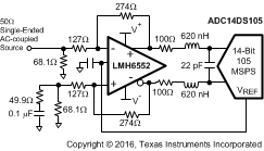
With external gain set resistors and integrated common mode feedback, the LMH6552 can be configured as either a differential input to differential output or single-ended input to differential output gain block. The LMH6552 can be AC- or DC-coupled at the input which makes it suitable for a wide range of applications, including communication systems and high-speed oscilloscope front ends. The performance of the LMH6552 driving an ADC14DS105 device is 86 dBc SFDR and 74 dBc SNR up to 40 MHz.
The LMH6552 is available in an 8-pin SOIC package as well as a space-saving, thermally enhanced 8-pin WSON package for higher performance.
Device Information(1)
| PART NUMBER | PACKAGE | BODY SIZE (NOM) |
|---|---|---|
| LMH6552 | SOIC (8) | 4.90 mm × 3.91 mm |
| WSON (8) | 3.00 mm × 2.50 mm |
- For all available packages, see the orderable addendum at the end of the datasheet.
Typical Application Schematic
