SNOSC61C January 2012 – September 2014 LMH6642Q-Q1 , LMH6643Q-Q1
PRODUCTION DATA.
- 1 Features
- 2 Applications
- 3 Description
- 4 Revision History
- 5 Description (continued)
- 6 Pin Configuration and Functions
- 7 Specifications
- 8 Application and Implementation
- 9 Device and Documentation Support
- 10Mechanical, Packaging, and Orderable Information
Package Options
Mechanical Data (Package|Pins)
- DBV|5
Thermal pad, mechanical data (Package|Pins)
Orderable Information
1 Features
- (VS = ±5 V, TA = 25°C, RL = 2 kΩ, AV = +1. Typical Values Unless Specified).
- −3dB BW (AV = +1) 130 MHz
- Supply Voltage Range 2.7 V to 10 V
- Slew Rate, (AV = −1) 130V/µs(1)
- Supply Current (no load) 2.7 mA/amp
- Output Short Circuit Current +115 mA/−145 mA
- Linear Output Current ±75mA
- Input Common Mode Voltage 0.5V Beyond V−, 1V from V+
- Output Voltage Swing 40mV from Rails
- Input Voltage Noise (100kHz) 17nV/√Hz
- Input Current Noise (100kHz) 0.9pA/√Hz
- THD (5MHz, RL = 2 kΩ, VO = 2VPP, AV = +2) −62 dBc
- Settling Time 68ns
- Fully Characterized for 3 V, 5 V, and ±5 V
- Overdrive Recovery 100ns
- Output Short Circuit Protected(2)
- No Output Phase Reversal with CMVR Exceeded
- LMH6643QMM and LMH6642QMF are AEC-Q100 Grade 3 Qualified and are Manufactured on an Automotive Grade Flow
2 Applications
- Active Filters
- CD/DVD ROM
- ADC Buffer Amp
- Portable Video
- Current Sense Buffer
- Automotive
3 Description
The LMH664X family true single supply voltage feedback amplifiers offer high speed (130 MHz), low distortion (−62 dBc), and exceptionally high output current (approximately 75 mA) at low cost and with reduced power consumption when compared against existing devices with similar performance.
Input common mode voltage range extends to 0.5 V below V− and 1 V from V+. Output voltage range extends to within 40mV of either supply rail, allowing wide dynamic range especially desirable in low voltage applications. The output stage is capable of approximately 75 mA in order to drive heavy loads. Fast output Slew Rate (130 V/µs) ensures large peak-to-peak output swings can be maintained even at higher speeds, resulting in exceptional full power bandwidth of 40 MHz with a 3-V supply. These characteristics, along with low cost, are ideal features for a multitude of industrial and commercial applications.
Device Information(1)
| PART NUMBER | PACKAGE | BODY SIZE (NOM) |
|---|---|---|
| LMH6642-Q1 | SOT-23 (5) | 2.90 mm × 1.60 mm |
| LMH6643-Q1 | VSSOP (8) | 3.00 mm × 3.00 mm |
- For all available packages, see the orderable addendum at the end of the datasheet.
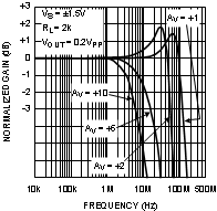
Closed Loop Gain vs. Frequency for Various Gain
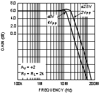
Large Signal Frequency Response