SNOS956E June 2001 – August 2014 LMH6654 , LMH6655
PRODUCTION DATA.
- 1 Features
- 2 Applications
- 3 Description
- 4 Revision History
- 5 Pin Configuration and Functions
- 6 Specifications
- 7 Application and Implementation
- 8 Power Supply Recommendations
- 9 Layout
- 10Device and Documentation Support
- 11Mechanical, Packaging, and Orderable Information
Package Options
Mechanical Data (Package|Pins)
Thermal pad, mechanical data (Package|Pins)
Orderable Information
1 Features
- (VS = ±5 V, TJ = 25 °C, Typical Values Unless Specified)
- Voltage Feedback Architecture
- Unity Gain Bandwidth 250 MHz
- Supply Voltage Range ±2.5V to ±6V
- Slew Rate 200 V/µsec
- Supply Current 4.5 mA/channel
- Input Common Mode Voltage −5.15V to +3.7V
- Output Voltage Swing (RL = 100 Ω) −3.6V to 3.4V
- Input Voltage Noise 4.5 nV/√Hz
- Input Current Noise 1.7 pA/√Hz
- Settling Time to 0.01% 25 ns
2 Applications
- ADC Drivers
- Consumer Video
- Active Filters
- Pulse Delay Circuits
- xDSL Receiver
- Pre-amps
3 Description
The LMH6654 and LMH6655 single and dual high speed voltage feedback amplifiers are designed to have unity-gain stable operation with a bandwidth of 250 MHz. They operate from ±2.5 V to ±6 V and each channel consumes only 4.5 mA. The amplifiers feature very low voltage noise and wide output swing to maximize signal-to-noise ratio, and possess a true single supply capability with input common mode voltage range extending 150 mV below negative rail and within 1.3 V of the positive rail. The high speed and low power combination of the LMH6654 and LMH6655 make these products an ideal choice for many portable, high speed applications where power is at a premium.
The LMH6654 and LMH6655 are built on TI’s Advance VIP10™ (Vertically Integrated PNP) complementary bipolar process.
The LMH6654 is packaged in 5-Pin SOT-23 and 8-Pin SOIC. The LMH6655 is packaged in 8-Pin VSSOP (DGK) and 8-Pin SOIC.
Device Information(1)
| PART NUMBER | PACKAGE | BODY SIZE (NOM) |
|---|---|---|
| LMH6654 | SOIC (8) | 4.90 mm x 3.91 mm |
| LMH6654 | SOT-23 (5) | 2.90 mm x 1.60 mm |
| LMH6655 | SOIC (8) | 4.90 mm x 3.91 mm |
| LMH6655 | VSSOP (8) | 3.00 mm x 3.00 mm |
- For all available packages, see the orderable addendum at the end of the datasheet.
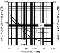
3.1 Input Voltage and Curernt Noise vs. Frequency (Vs= ±5V)
4 Revision History
Changes from D Revision (March 2013) to E Revision
- Changed data sheet structure and organization. Added, updated, or renamed the following sections: Device Information Table, Application and Implementation; Power Supply Recommendations; Device and Documentation Support; Mechanical, Packaging, and Ordering Information. Deleted Switching Characteristics due to redundancy. Go
- Changed from Junction Temperature Range to "Operating Temperature Range"Go
- Deleted TJ = 25°CGo
- Deleted TJ = 25°C Go
Changes from C Revision (March 2013) to D Revision
- Changed layout of National Data Sheet to TI formatGo