SNOS956E June 2001 – August 2014 LMH6654 , LMH6655
PRODUCTION DATA.
- 1 Features
- 2 Applications
- 3 Description
- 4 Revision History
- 5 Pin Configuration and Functions
- 6 Specifications
- 7 Application and Implementation
- 8 Power Supply Recommendations
- 9 Layout
- 10Device and Documentation Support
- 11Mechanical, Packaging, and Orderable Information
Package Options
Mechanical Data (Package|Pins)
Thermal pad, mechanical data (Package|Pins)
Orderable Information
7 Application and Implementation
7.1 Application Information
The LMH6654 single and LMH6655 dual high speed, voltage feedback amplifiers are manufactured on TI’s new VIP10™ (Vertically Integrated PNP) complementary bipolar process. These amplifiers can operate from ±2.5 V to ±6 V power supply. They offer low supply current, wide bandwidth, very low voltage noise and large output swing. Many of the typical performance plots found in the datasheet can be reproduced if 50 Ω coax and 50 Ω RIN/ROUT resistors are used.
7.2 Typical Application
7.2.1 Design Requirements
7.2.1.1 Components Selection and Feedback Resistor
It is important in high-speed applications to keep all component leads short since wires are inductive at high frequency. For discrete components, choose carbon composition axially leaded resistors and micro type capacitors. Surface mount components are preferred over discrete components for minimum inductive effect. Never use wire wound type resistors in high frequency applications.
Large values of feedback resistors can couple with parasitic capacitance and cause undesired effects such as ringing or oscillation in high-speed amplifiers. Keep resistors as low as possible consistent with output loading consideration. For a gain of 2 and higher, 402 Ω feedback resistor used for the typical performance plots gives optimal performance. For unity gain follower, a 25 Ω feedback resistor is recommended rather than a direct short. This effectively reduces the Q of what would otherwise be a parasitic inductance (the feedback wire) into the parasitic capacitance at the inverting input.
7.2.2 Detailed Design Procedure
7.2.2.1 Driving Capacitive Loads
Capacitive loads decrease the phase margin of all op amps. The output impedance of a feedback amplifier becomes inductive at high frequencies, creating a resonant circuit when the load is capacitive. This can lead to overshoot, ringing and oscillation. To eliminate oscillation or reduce ringing, an isolation resistor can be placed as shown in Figure 40 below. At frequencies above

the load impedance of the Amplifier approaches RISO. The desired performance depends on the value of the isolation resistor. The isolation resistance vs. capacitance load graph in the typical performance characteristics provides the means for selection of the value of RS that provides ≤ 3 dB peaking in closed loop AV = 1 response. In general, the bigger the isolation resistor, the more damped the pulse response becomes. For initial evaluation, a 50Ω isolation resistor is recommended.
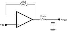 Figure 40. Isolation Resistor Placement
7.2.2.2 Bias Current Cancellation
In order to cancel the bias current errors of the non-inverting configuration, the parallel combination of the gain setting Rg and feedback Rf resistors should equal the equivalent source resistance Rseq as defined in Figure 41. Combining this constraint with the non-inverting gain equation, allows both Rf and Rg to be determined explicitly from the following equations:
For inverting configuration, bias current cancellation is accomplished by placing a resistor Rb on the non-inverting input equal in value to the resistance seen by the inverting input (Rf//(Rg+Rs). The additional noise contribution of Rb can be minimized through the use of a shunt capacitor.
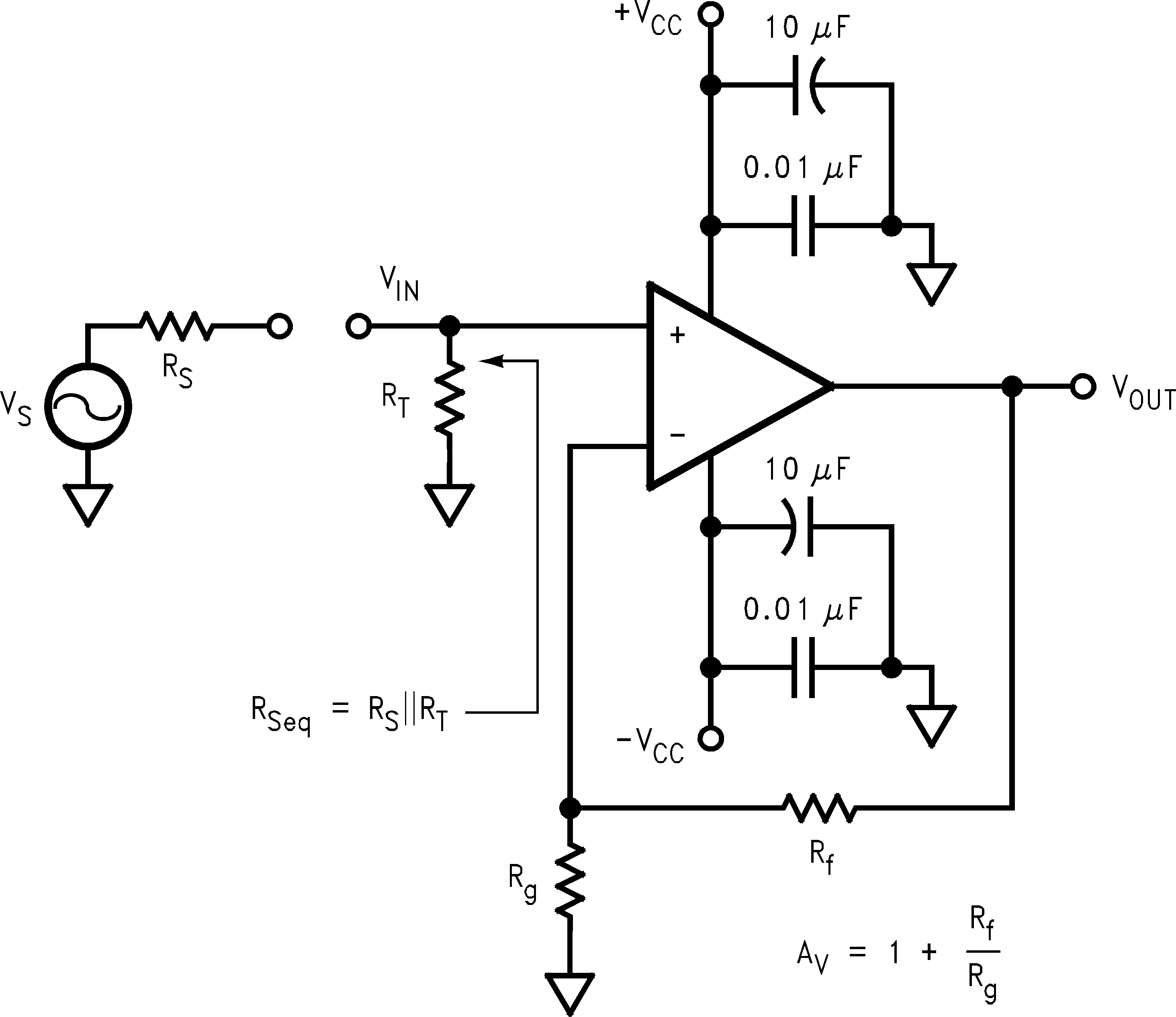 Figure 41. Non-Inverting Amplifier Configuration
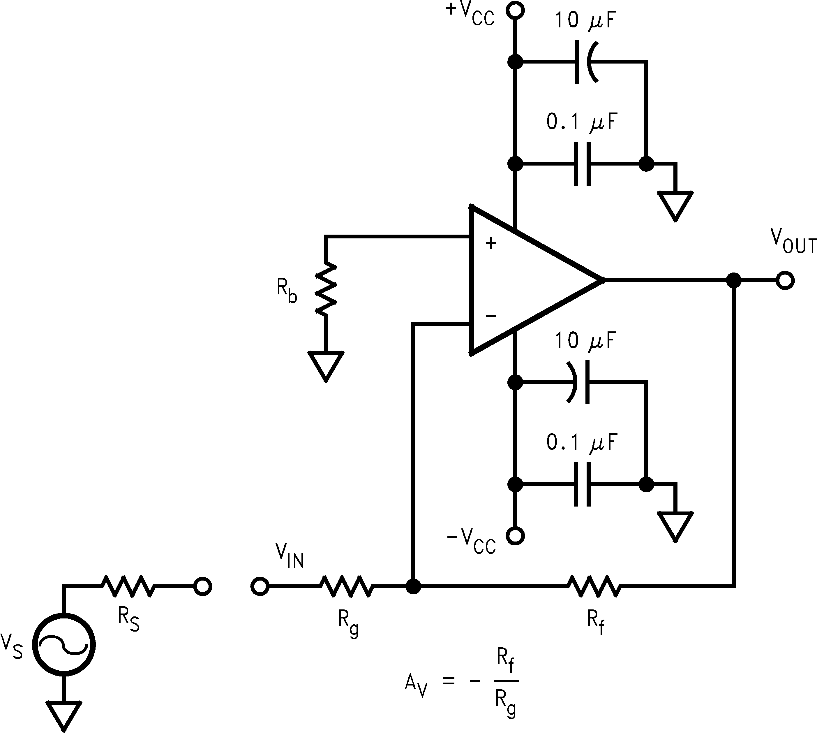 Figure 42. Inverting Amplifier Configuration
7.2.2.3 Total Input Noise vs. Source Resistance
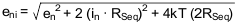
The noise model for the non-inverting amplifier configuration showing all noise sources is described in Figure 43. In addition to the intrinsic input voltage noise (en) and current noise (in = in+ = in−) sources, there also exits thermal voltage noise  associated with each of the external resistors. Equation 3 provides the general form for total equivalent input voltage noise density (eni). Equation 4 is a simplification of Equation 3 that assumes Rf || Rg = Rseq for bias current cancellation. Figure 44 illustrates the equivalent noise model using this assumption. The total equivalent output voltage noise (eno) is eni * AV.
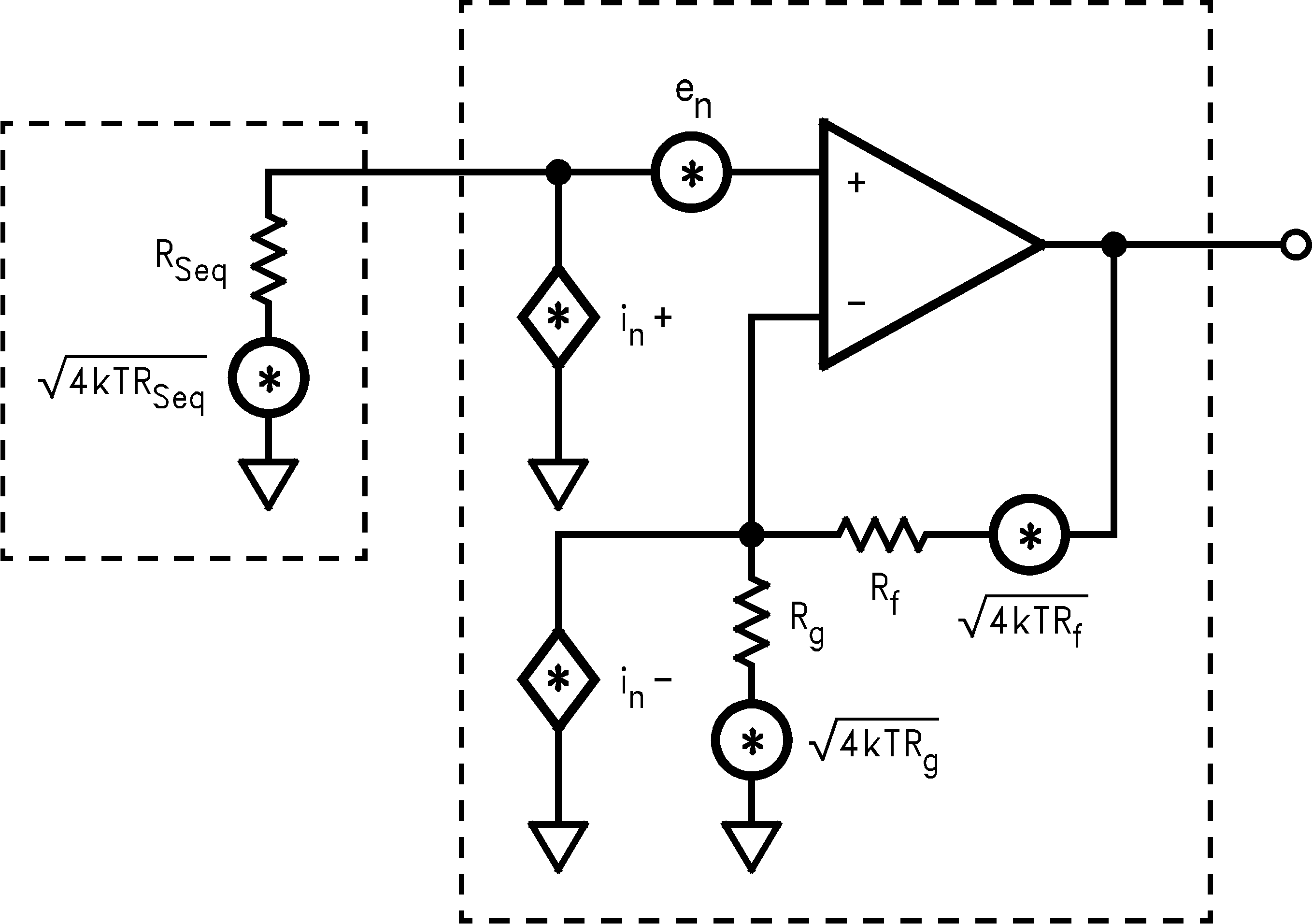 Figure 43. Non-Inverting Amplifier Noise Model

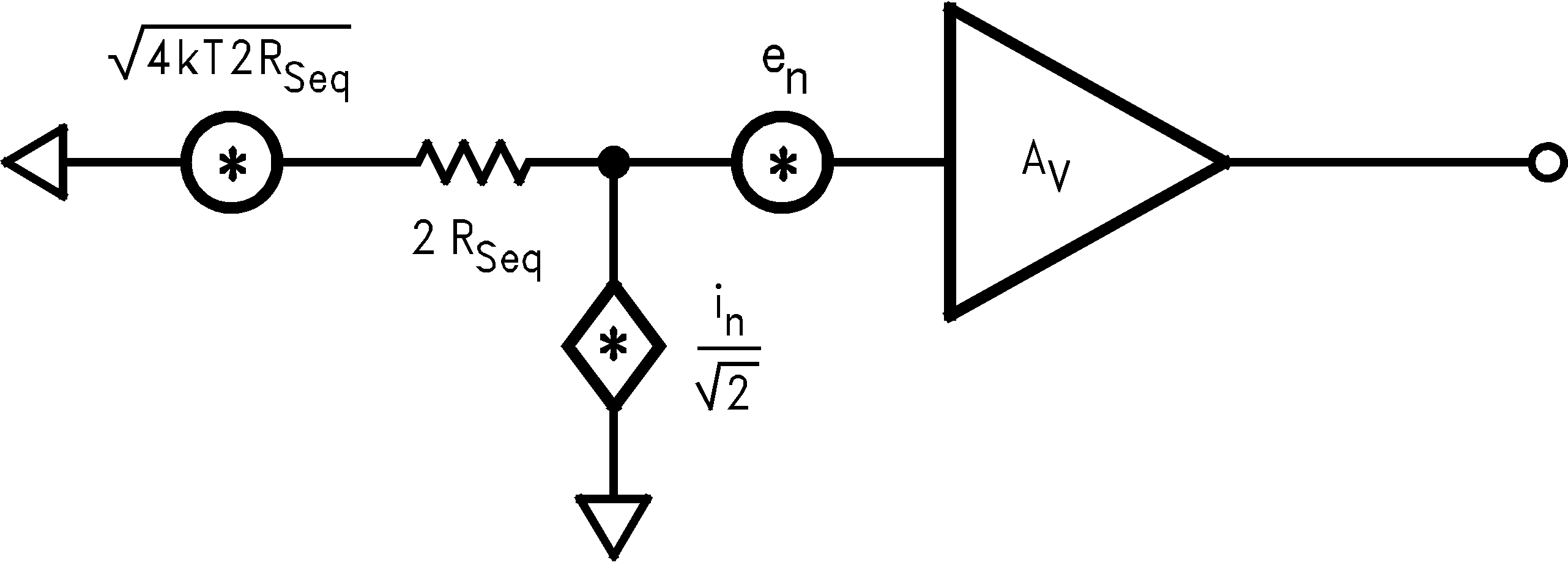 Figure 44. Noise Model with Rf || Rg = Rseq
If bias current cancellation is not a requirement, then Rf || Rg does not need to equal Rseq. In this case, according to Equation 3, Rf and Rg should be as low as possible in order to minimize noise. Results similar to Equation 3 are obtained for the inverting configuration on if Rseq is replaced by Rb || Rg is replaced by Rg + Rs. With these substitutions, Equation 3 will yield an eni referred to the non-inverting input. Referring eni to the inverting input is easily accomplished by multiplying eni by the ratio of non-inverting to inverting gains.
7.2.2.3.1 Noise Figure
Noise Figure (NF) is a measure of the noise degradation caused by an amplifier.
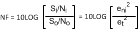
The noise figure formula is shown in Equation 5. The addition of a terminating resistor RT, reduces the external thermal noise but increases the resulting NF.
The NF is increased because the RT reduces the input signal amplitude thus reducing the input SNR.
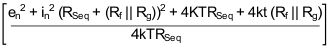
The noise figure is related to the equivalent source resistance (Rseq) and the parallel combination of Rf and Rg. To minimize noise figure, the following steps are recommended:
- Minimize Rf||Rg
- Choose the Optimum Rs (ROPT)
ROPT is the point at which the NF curve reaches a minimum and is approximated by: