SNOS956E June 2001 – August 2014 LMH6654 , LMH6655
PRODUCTION DATA.
- 1 Features
- 2 Applications
- 3 Description
- 4 Revision History
- 5 Pin Configuration and Functions
- 6 Specifications
- 7 Application and Implementation
- 8 Power Supply Recommendations
- 9 Layout
- 10Device and Documentation Support
- 11Mechanical, Packaging, and Orderable Information
Package Options
Mechanical Data (Package|Pins)
Thermal pad, mechanical data (Package|Pins)
Orderable Information
9 Layout
9.1 Layout Guidelines
With all high frequency devices, board layouts with stray capacitance have a strong influence on the AC performance. The LMH6654/LMH6655 are not exception and the inverting input and output pins are particularly sensitive to the coupling of parasitic capacitance to AC ground. Parasitic capacitances on the inverting input and output nodes to ground could cause frequency response peaking and possible circuit oscillation. Therefore, the power supply, ground traces and ground plan should be placed away from the inverting input and output pins. Also, it is very important to keep the parasitic capacitance across the feedback to an absolute minimum.
The PCB should have a ground plane covering all unused portion of the component side of the board to provide a low impedance path. All trace lengths should be minimized to reduce series inductance.
Supply bypassing is required for the amplifiers performance. The bypass capacitors provide a low impedance return current path at the supply pins. They also provide high frequency filtering on the power supply traces. It is recommended that a ceramic decoupling capacitor 0.1 µF chip should be placed with one end connected to the ground plane and the other side as close as possible to the power pins. An additional 10 µF tantalum electrolytic capacitor should be connected in parallel, to supply current for fast large signal changes at the output.
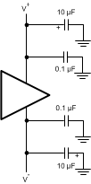 Figure 45. Supply Bypass Capacitors
9.1.1 Evaluation Boards
TI provides the following evaluation boards as a guide for high frequency layout and as an aid in device testing and characterization.
| DEVICE | PACKAGE | EVALULATION BOARD PN |
|---|---|---|
| LMH6654MF | 5-Pin SOT-23 | LMH730216 |
| LMH6654MA | 8-Pin SOIC | LMH730227 |
| LMH6655MA | 8-Pin SOIC | LMH730036 |
| LMH6655MM | 8-Pin VSSOP (DGK) | LMH730123 |
Components Needed to Evaluate the LMH6654 on the LMH730227 Evaluation Board:
- Rf, Rg use the datasheet to select values.
- RIN, ROUT typically 50 Ω (Refer to the Basic Operation section of the evaluation board datasheet for details)
- Rf is an optional resistor for inverting again configurations (select Rf to yield desired input impedance = Rg||Rf)
- C1, C2 use 0.1 µF ceramic capacitors
- C3, C4 use 10 µF tantalum capacitors
Components not used:
1. C5, C6, C7, C8
2. R1 thru R8
The evaluation boards are designed to accommodate dual supplies. The board can be modified to provide single operation. For best performance;
1) Do not connect the unused supply.
2) Ground the unused supply pin.