SNOS956E June 2001 – August 2014 LMH6654 , LMH6655
PRODUCTION DATA.
- 1 Features
- 2 Applications
- 3 Description
- 4 Revision History
- 5 Pin Configuration and Functions
- 6 Specifications
- 7 Application and Implementation
- 8 Power Supply Recommendations
- 9 Layout
- 10Device and Documentation Support
- 11Mechanical, Packaging, and Orderable Information
Package Options
Mechanical Data (Package|Pins)
Thermal pad, mechanical data (Package|Pins)
Orderable Information
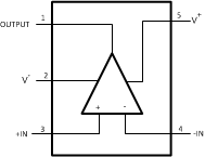
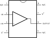
5 Pin Configuration and Functions
Package DBV
5-Pin (LMH6654)
Top View
Package D
8-Pin (LMH6654)
Top View
SOIC and VSSOP (DGK)
8-Pin (LMH6655)
Top View
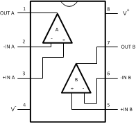
Pin Functions
| PIN | I/O | DESCRIPTION | ||||
|---|---|---|---|---|---|---|
| NAME | LMH6654 | LMH6655 | ||||
| DBV | D | DGK | ||||
| -IN | 4 | 2 | I | Inverting Input | ||
| +IN | 3 | 3 | I | Non-inverting Input | ||
| -IN A | 2 | I | ChA Inverting Input | |||
| +IN A | 3 | I | ChA Non-inverting Input | |||
| -IN B | 6 | I | ChB Inverting Input | |||
| +IN B | 5 | I | ChB Non-inverting Input | |||
| N/C | 1, 5, 8 | –– | No Connection | |||
| OUT A | 1 | O | ChA Output | |||
| OUT B | 7 | O | ChB Output | |||
| OUTPUT | 1 | 6 | O | Output | ||
| V- | 2 | 4 | 4 | I | Negative Supply | |
| V+ | 5 | 7 | 8 | I | Positive Supply | |