SNOSAI9I September 2005 – November 2015 LMP7701 , LMP7702 , LMP7704
PRODUCTION DATA.
- 1 Features
- 2 Applications
- 3 Description
- 4 Revision History
- 5 Description (continued)
- 6 Pin Configuration and Functions
- 7 Specifications
- 8 Detailed Description
- 9 Application and Implementation
- 10Power Supply Recommendations
- 11Layout
- 12Device and Documentation Support
- 13Mechanical, Packaging, and Orderable Information
Package Options
Mechanical Data (Package|Pins)
Thermal pad, mechanical data (Package|Pins)
Orderable Information
11 Layout
11.1 Layout Guidelines
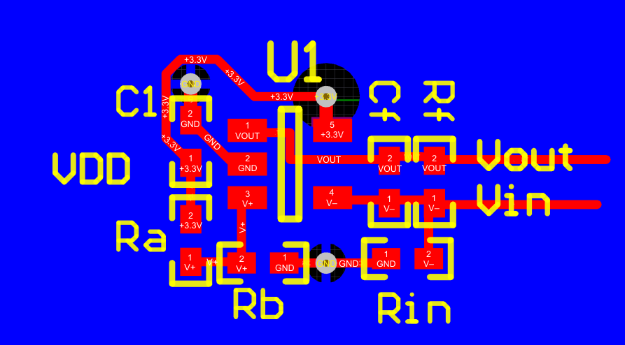
Take care to minimize the loop area formed by the bypass capacitor connection between supply pins and ground. A ground plane underneath the device is recommended; any bypass components to ground should have a nearby via to the ground plane. The optimum bypass capacitor placement is closest to the corresponding supply pin. Use of thicker traces from the bypass capacitors to the corresponding supply pins will lower the power supply inductance and provide a more stable power supply.
The feedback components should be placed as close to the device as possible to minimize stray parasitics.
11.2 Layout Example
 Figure 52. LMP7701 Example Layout