SNVS829E March 1999 – February 2017 LMP8480 , LMP8481
PRODUCTION DATA.
- 1 Features
- 2 Applications
- 3 Description
- 4 Revision History
- 5 Device Comparison Table
- 6 Pin Configuration and Functions
- 7 Specifications
-
8 Detailed Description
- 8.1 Overview
- 8.2 Functional Block Diagrams
- 8.3
Feature Description
- 8.3.1 Basic Connections
- 8.3.2 Selection of the Sense Resistor
- 8.3.3 Using PCB Traces as Sense Resistors
- 8.3.4 VREFA and VREFB Pins (LMP8481 Only)
- 8.3.5 Reference Input Voltage Limits (LMP8481 Only)
- 8.3.6 Low-Side Current Sensing
- 8.3.7 Input Series Resistance
- 8.3.8 Minimum Output Voltage
- 8.3.9 Swinging Output Below Ground
- 8.3.10 Maximum Output Voltage
- 8.4 Device Functional Modes
- 9 Application and Implementation
- 10Power Supply Recommendations
- 11Layout
- 12Device and Documentation Support
- 13Mechanical, Packaging, and Orderable Information
Package Options
Mechanical Data (Package|Pins)
- DGK|8
Thermal pad, mechanical data (Package|Pins)
- DGK|8
Orderable Information
8 Detailed Description
8.1 Overview
The LMP8480 and LMP8481 are single-supply, high-side current sense amplifiers with available fixed gains of x20, x60 and x100. The power supply range is 4.5 V to 76 V, and the common-mode input voltage range is capable of 4.0-V to 76-V operation. The supply voltage and common-mode range are completely independent of each other, which causes the LMP848x supply voltage to be extremely flexible because the LMP848x supply voltage can be greater than, equal to, or less than the load source voltage, and allows the device to be powered from the system supply or the load supply voltage.
The LMP8480 and LMP8481 supply voltage does not have to be larger than the load source voltage. A 76-V load source voltage with a 5-V supply voltage is perfectly acceptable.
8.1.1 Theory of Operation
The LMP8480 and LMP8481 are comprised of two main stages. The first stage is a differential input current to voltage converter, followed by a differential voltage amplifier and level-shifting output stage. Also present is an internal 14-V low-dropout regulator (LDO) to power the amplifiers and output stage, as well as a reference divider resistor string to allow the setting of the reference level.
As Figure 18 illustrates, the current flowing through RSENSE develops a voltage drop called VSENSE. The voltage across the sense resistor, VSENSE, is then applied to the input RSP and RSN pins of the amplifier.
Internally, the voltage on each input pin is converted to a current by the internal precision thin-film input resistors RGP and RGN. A second set of much higher value VCM sense resistors between the inputs provide a sample of the input common-mode voltage for internal use by the differential amplifier.
VSENSE is applied to the differential amplifier through RGP and RGN. These resistors change the input voltage to a differential current. The differential amplifier then servos the resistor currents through the MOSFETs to maintain a zero balance across the differential amplifier inputs.
With no input signal present, the currents in RGP and RGN are equal. When a signal is applied to VSENSE, the current through RGP and RGN are imbalanced and are no longer equal. The amplifier then servos the MOSFETS to correct this current imbalance, and the extra current required to balance the input currents is then reflected down into the two lower 400-kΩ tail resistors. The difference in the currents into the tail resistors is therefore proportional to the amplitude and polarity of VSENSE. The tail resistors, being larger than the input resistors for the same current, then provide voltage gain by changing the current into a proportionally larger voltage. The gain of the first stage is then set by the tail resistor value divided by RG value.
The differential amplifier stage then samples the voltage difference across the two 400-kΩ tail resistors and also applies a further gain-of-five and output level-shifting according to the applied reference voltage (VREF).
The resulting output of the amplifier will be equal to the differential input voltage times the gain of the device, plus any voltage value applied to the two VREF pins.
The resistor values in the schematic are ideal values for clarity and understanding. Table 1 shows the actual values used that account for parallel combinations and loading. This table can be used for calculating the effects of any additional external resistance.
The LMP8480 is identical to the LMP8481, except that both the VREF pins are grounded internally.
Table 1. Actual Internal Resistor Values
| GAIN OPTION | RGP AND RGN
(Each) |
RVCMSENSE
(Each) |
RTAIL
(Each) |
DIFFERENTIAL AMP FB (Each) |
VREFx RESISTORS (Each) |
|---|---|---|---|---|---|
| 20x | 98.38 k | 491.9 k | 393.52 k | 1967.6 k | 98.38 k |
| 60x | 32.793 k | 172.165 k | 393.52 k | 1967.6 k | 98.38 k |
| 100x | 19.676 k | 98.38 k | 393.52 k | 1967.6 k | 98.38 k |
8.2 Functional Block Diagrams
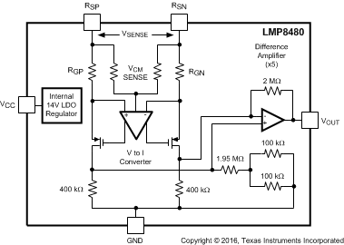 Figure 17. LMP8480 Block Diagram
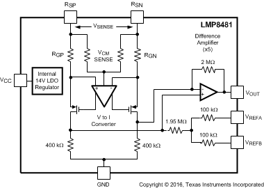 Figure 18. LMP8481 Block Diagram
8.3 Feature Description
8.3.1 Basic Connections
Figure 19 through Figure 22 show the basic connections for several different configurations.
Figure 19 shows the basic connections for the LMP8480 for unidirectional applications. The output is at zero with zero sense voltage.
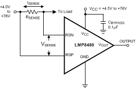 Figure 19. LMP8480 Basic Connections (Unidirectional)
Figure 20 shows the basic connections for the LMP8481 for bidirectional applications using an external reference input. At zero input voltage, the output is at the applied reference voltage (VREF), moving positive or negative from the zero reference point.
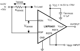 Figure 20. LMP8481 Basic Connections for External 1:1 VREF Input (Bidirectional)
Figure 21 shows the basic connections for the LMP8481 for bidirectional applications centering the output at one-half the applied VREF or VCC voltage. If VREFA is connected to VCC, then the output zero point is VCC / 2. If VREFA is connected to the ADC VREF line, then the zero output is at mid-scale for the ADC.
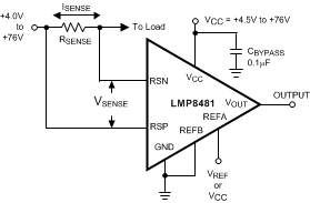 Figure 21. LMP8481 Basic Connections for Mid-Bias (VREF / 2) Input (Bidirectional)
Figure 22 shows the how to connect the LMP8481 for unidirectional applications, thus making the LMP8481 equivalent to the LMP8480 in Figure 19.
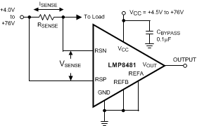 Figure 22. LMP8481 Connections for Unidirectional Configuration (Equivalent to LMP8480 Unidirectional)
8.3.2 Selection of the Sense Resistor
The accuracy of the current measurement depends heavily on the accuracy of the shunt resistor RSENSE. The value of RSHUNT depends on the application and is a compromise between small-signal accuracy, maximum permissible voltage drop, and allowable power dissipation in the current measurement circuit.
The use of a 4-terminal or Kelvin sense resistor is highly recommended; see the Layout Guidelines section.
For best results, the value of the resistor is calculated from the maximum expected load current ILMAX and the expected maximum output swing VOUTMAX, plus a few percent of headroom. See the Maximum Output Voltage section for details about the maximum output voltage limits.
High values of RSENSE provide better accuracy at lower currents by minimizing the effects of amplifier offset. Low values of RSENSE minimize load voltage loss, but at the expense of accuracy at low currents. A compromise between low current accuracy and load circuit losses must generally be made.
The maximum VSENSE voltage that must be generated across the RSENSE resistor is shown in Equation 1:
NOTE
The maximum VSENSE voltage must be no more than 667 mV.
From this maximum VSENSE voltage, the RSENSE value can be calculated from Equation 2:
Take care not exceed the maximum power dissipation of the resistor. The maximum sense resistor power dissipation is shown in Equation 3:
Using a 2-3x minimum safety margin is recommended in selecting the power rating of the resistor.
8.3.3 Using PCB Traces as Sense Resistors
While it may be tempting to use a known length of PCB trace resistance as a sense resistor, it is not recommended.
The temperature coefficient of copper is typically 3300-4000 ppm/°K, and can vary over PCB process variations and require measurement correction (possibly requiring ambient temperature measurements).
A typical surface mount sense resistor tempco is in the 50 ppm to 500 ppm/°C range offering more measurement consistency and accuracy over the copper trace. Special low-tempco resistors are available in the 0.1 to 50 ppm range, but at a higher cost.
8.3.4 VREFA and VREFB Pins (LMP8481 Only)
The voltage applied to the VREFA and VREFB pins controls the output zero reference level. Depending on how the pins are configured, the output reference level can be set to GND, or VCC / 2, or external VREF / 2, or the average of two different input references.
The reference inputs consist of a pair of divider resistors with equal values to a common summing point, VREF', as shown in Figure 23. Assuming VSENSE is zero, the output is at the same value as VREF'.
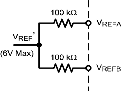 Figure 23. VREF Input Resistor Network
VREF' is the voltage at the resistor tap-point that is directly applied to the output as an offset. With the two VREF inputs tied together, the output zero voltage has a 1:1 ratio relationship with VREF.
Where:
or:
8.3.4.1 One-to-One (1:1) Reference Input
To directly set the reference level, the two inputs are connected to the external reference voltage. The applied VREF is reflected 1:1 on the output, as shown in Figure 24.
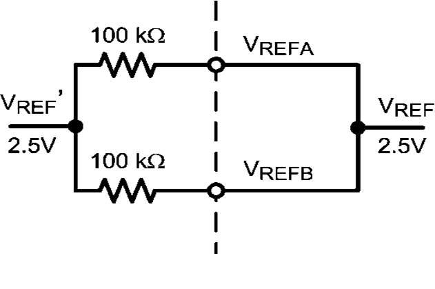 Figure 24. Applying 1:1 Direct Reference Voltage
8.3.4.2 Setting Output to One-Half VCC or external VREF
For mid-range operation, VREFB must be tied to ground and VREFA can be tied to VCC or an external A/D reference voltage. The output is set to one-half the reference voltage. For example, a 5-V reference results in a 2.5-V output zero reference.
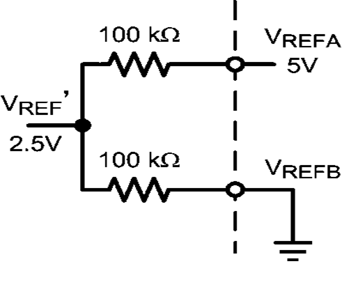 Figure 25. Applying a Divided Reference Voltage
When the reference pins are biased at different voltages, the output is referenced to the average of the two applied voltages.
The reference pins must always be driven from clean, stable sources, such as A/D reference lines or clean supply lines. Any noise or drifts on the reference inputs are directly reflected in the output. Take care if the power supply is used as the reference source so as to not introduce supply noise, drift or sags into the measurement.
Different resistor divider ratios can be set by adding external resistors in series with the internal 100-kΩ resistors, though the temperature coefficient (tempco) of the external resistors may not tightly track the internal resistors and there are slight errors over temperature.
The LMP8480 is identical to the LMP8481, except that both the VREF pins are grounded internally. The LMP8481 can replace the LMP8480 if both VREF pins are grounded.
8.3.5 Reference Input Voltage Limits (LMP8481 Only)
The maximum voltage on either reference input pin is limited to VCC or 12 V, whichever is less.
The average voltage on the two VREF pins, and thus the actual output reference voltage level, is limited to a maximum of 1.5 V below VCC, or 6 V, whichever is less. Beware that supply voltages of less than 7.5 V have a diminishing VREF maximum.
Both VREFA and VREFB can both be grounded to provide a ground referenced output (thus functionally duplicating the LMP8480).
Note that there can be a dynamic error in the VREF to output level matching of up to 100 µV/V. Normally this error is not an issue for fixed references, but if the reference voltage is dynamically adjusted during operation, this error must be taken into account during calibration routines. This error varies in both amplitude and polarity part-to-part, but the slope is generally linear.
8.3.6 Low-Side Current Sensing
The LMP8480 and LMP8481 are not recommended for low-side current sensing at ground level. The voltage on either input pin must be a minimum of 4.0 V above the ground pin for proper operation. The output level may not be valid for common-mode voltages below 4 V. This minimum voltage requirement must be taken into consideration for monitoring or feedback applications where the load-supply voltage can dip below 4 V or be switched completely off.
8.3.7 Input Series Resistance
Because the input stage uses precision resistors to convert the voltage on the input pin to a current, any resistance added in series with the input pins changes the gain. If a resistance is added in series with an input, the gain of that input does not track that of the other input, causing a constant gain error.
TI does not recommend using external resistances to alter the gain because external resistors do not have the same thermal matching as the internal thin film resistors.
If resistors are purposely added for filtering, resistance must be added equally to both inputs and the user must be aware that the gain changes slightly. See the end of the Theory of Operation section for the internal resistor values. External resistances must be kept below 10 Ω.
8.3.8 Minimum Output Voltage
The amplifier output cannot swing to exactly 0 V. There is always a minimum output voltage set by the output transistor saturation and input offset errors. This voltage creates a minimum output swing around the zero current reading resulting from the output saturation. The user must be aware of this output swing when designing any servo loops or data acquisition systems that may assume 0 V = 0 A. If a true zero is required, use the LMP8481 with a VREF set slightly above ground (> 50 mV); see the Swinging Output Below Ground section for a possible solution to this issue.
8.3.9 Swinging Output Below Ground
If a negative supply is available, a pulldown resistor can be added from the output to the negative voltage to allow the output to swing a few millivolts below ground. Adding a pulldown resistor allows the ADC to resolve true zero and recover codes that normally are lost to the negative output saturation limit.
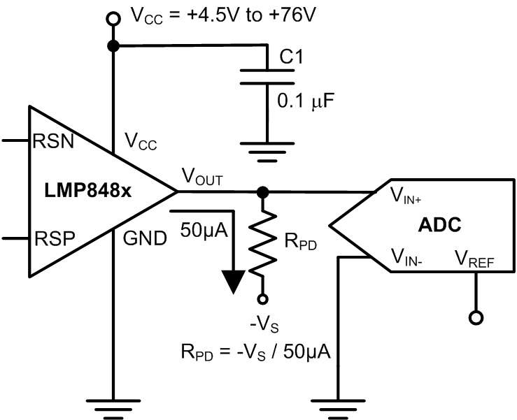 Figure 26. Output Pulldown Resistor Example
A minimum of 50 µA must be sourced (pulled) from the output to a negative voltage. The pulldown resistor can be calculated from:
For example, if a –5-V supply is available, use a pulldown resistor of 5 V / 50 µA = 100 kΩ. Adding this resistor allows the output to swing to approximately 10 mV below ground.
This technique can also reduce the maximum positive swing voltage. Do not forget to include the parallel loading effects of the pulldown any output load. Exceeding –100 mV on the output is not recommended. Source currents greater than 100 µA must be avoided to prevent self-heating at high-supply voltages. Pulldown resistor values must not be so low as to heavily load the output during positive output excursions. This mode of operation is not directly specified and is not ensured.
8.3.10 Maximum Output Voltage
The LMP8481 has an internal precision 14-V low-dropout regulator that limits the maximum amplifier output swing to approximately 250 mV below VCC or 13.7 V (whichever is less). This regulator effectively clamps the maximum output to slightly less than 13.7 V even with a VCC greater than 14 V; see Typical Application With a Resistive Divider section for more information.
8.4 Device Functional Modes
8.4.1 Unidirectional vs Bidirectional Operation
Unidirectional operation is where the load current only flows in one direction (VSENSE is always positive). Application examples are PA monitoring, non-inductive load monitoring, and laser or LED drivers. Unidirectional operation allows the output zero reference to be true zero volts on the output. The LMP8480 is designed for unidirectional applications where the setting of VREF is not required; see the Unidirectional Application With the LMP8480 section for more details.
Bidirectional operation is where the load current can flow in both directions (VSENSE can be positive or negative). Application examples are battery-charging or regenerative motor monitoring. The LMP8481 is designed for bidirectional applications and has a pair of VREF pins to allow the setting of the output zero reference level (VREF); see the Unidirectional Application With the LMP8480 section for more details.