7.3 Feature Description
7.3.1 Current Sense Input Channel
The current sensing channel of the LMP92064 has a high impedance differential amplifier followed by a 12-bit analog-to-digital converter. The binary code result of a conversion is stored as a right-justified 16-bit number as shown in Table 1, where the 4 most significant bits are always 0. Due to an offset auto-calibration feature of the current sense channel path, the top 256 codes are clipped at code 3840, denoted by the trailing zeros found in the equivalent binary code of the maximum positive input voltage.
The output data of the current sense channel is accessible on registers 0x0203 and 0x0202.
Table 1. Ideal Current Channel Input Voltages and Output Codes
| DESCRIPTION |
ANALOG VALUE |
DIGITAL OUTPUT |
| Full scale range |
V FS= 81.92 mV |
BINARY CODE
[B15:B0] |
HEX CODE |
| Least significant bit (LSB) |
VFS / 4096 |
| Maximum Positive Input Voltage |
VFS – 256 LSB |
0000 1111 0000 0000 |
0x0F00 |
| Zero |
0 V |
0000 0000 0000 0000 |
0x0000 |
7.3.2 Current Sense Input Channel Common-Mode and Differential Voltage Range (Dynamic Range Considerations)
The input voltage should be in the range of –0.2 V to 2 V. The input can withstand voltage up to VDD + 0.3 V absolute maximum but the operational range is limited to 2 V. Operation below –0.2 V or above 2 V on either input pin will introduce severe gain errors and nonlinearity.
The maximum differential voltage (defined as the voltage difference between INCP and INCN) for which the part is designed to work is 75 mV. Larger differential or common mode input voltages will not damage the part (as long as the input pins remain between GND – 0.3 V and VDD + 0.3 V), however, exposure for extended periods may affect device reliability. The ADC output code will not roll over and will clip at minimum or maximum scale when the maximum differential voltage is exceeded.
7.3.3 Voltage Sense Input Channel
The voltage sensing channel of the LMP92064 has a high impedance buffer amplifier followed by a 12-bit analog-to-digital converter. The binary code result of a conversion is also stored as a right-justified 16-bit number as shown in Table 2, where the 4 most significant bits are always 0.
The output data of the voltage sense channel is accessible on registers 0x0201 and 0x0200.
Table 2. Ideal Voltage Channel Input Voltages and Output Codes
| DESCRIPTION |
ANALOG VALUE |
DIGITAL OUTPUT |
| Full scale range |
V FS= 2.048 V |
BINARY CODE
[B15:B0] |
HEX CODE |
| Least significant bit (LSB) |
VFS / 4096 |
| Maximum Positive Input Voltage |
VFS – 1 LSB |
0000 1111 1111 1111 |
0x0FFF |
| Zero Code Voltage |
0 V |
0000 0000 0000 0000 |
0x0000 |
7.3.4 Reference
The LMP92064 includes an internal 2.048-V band-gap reference for the ADCs, which eliminates the need of an external reference and reduces component count and board space. The REFC pin is provided to allow bypassing this internal reference for low noise operation. A 1-µF ceramic decoupling capacitor is required between the REFC and REFG pins of the converter. The capacitor should be placed as close as possible to the pins of the device.
7.3.5 Reset
There are two methods to reset the LMP92064. A soft reset is done by setting bit7=1 in the CONFIG_A register. In a soft reset, the SPI state machine and the contents of registers 0x0000 and 0x0001 are unaffected.
A hardware reset is done by connecting the RESET pin of the LMP92064 to VDIG. If the pin is driven by a switch or a GPIO, TI recommends adding an external RC filter to prevent reset glitches.
7.3.6 Device Power-Up Sequence
The sources providing power to the analog and digital supply pins of the LMP92064, VDD and VDIG, must ramp up at the same time to have a proper power-on reset (POR) event. The easiest way to achieve it is to tie VDD and VDIG to the same power source using a star configuration.
7.4 Device Functional Modes
7.4.1 ADC Operation
The LMP92064 includes two 12-bit ADCs that are continuously running in the background. The device is configured, and data is read, using a four-wire SPI interface: CSB, SCLK, SDO and SDI. The device outputs its data on SDO, and the data for both channels is synchronized such that all data read would be from the same instant in time. New conversion data for both channels will only be made available after all registers are read in descending sequential order (addresses 0x0203-0x0200). All registers must be read otherwise new conversion data will not be available. Three different output data formats are available as detailed in Figure 20, Figure 21 and Figure 22.
The register address to read can automatically decrement if the CSB line is kept low longer. For example, to read all the conversion data, keep the CSB line low for 48 SPI clock cycles (16 clocks for command/address, 8 clocks for MSB of current channel, 8 clocks for LSB of current channel, 8 clocks for MSB of voltage channel and 8 clocks for LSB of voltage channel). The read command should start from address 0x0203.
7.5 Register Maps
- If written to, Reserved bits must be written to 0, unless otherwise indicated.
- Read back value of Reserved bits and registers is unspecified and should be discarded.
- Recommended values must be programmed and forbidden values must not be programmed where they are indicated in order to avoid unexpected results.
- If written to, registers indicated as Reserved must have the indicated default value as shown in the register map. Any other value can cause unexpected results.
Table 3. Register Map
| REGISTER NAME |
REGISTER DESCRIPTION |
ADDRESS |
ACCESS |
DEFAULT |
| CONFIG_A |
Interface Configuration A |
0x0000 |
R/W |
0x18 |
| CONFIG_B |
Interface Configuration B |
0x0001 |
R/W |
0x00 |
| Reserved |
Reserved |
0x0002 |
R/W |
0x00 |
| CHIP_TYPE |
Chip Type |
0x0003 |
RO |
0x07 |
| CHIP_ID |
Chip ID |
0x0004
0x0005 |
RO |
0x00
0x04 |
| CHIP_REV |
Chip Revision |
0x0006 |
RO |
0x01 |
| MFR_ID |
Manufacturer ID |
0x000C
0x000D |
RO |
0x51
0x04 |
| REG_UPDATE |
Register Update |
0x000F |
R/W |
0x00 |
| CONFIG_REG |
LMP92064 Specific Configuration Register |
0x0100 |
R/W |
0x00 |
| STATUS |
Status Register |
0x0103 |
RO |
N/A |
| DATA_VOUT |
Voltage Channel Output Data |
0x0200
0x0201 |
RO |
N/A |
| DATA_COUT |
Current Channel Output Data |
0x0202
0x0203 |
RO |
N/A |
Table 1. CONFIG_A: Interface Configuration A
| ADDR |
BIT 7 |
BIT 6 |
BIT 5 |
BIT 4 |
BIT 3 |
BIT 2 |
BIT 1 |
BIT 0 |
| 0x0000 |
RESET |
DDIR |
ADDRDIR |
SDDIR |
|
| [7] |
RESET(1) |
Soft reset (self-clearing) |
R/W |
|
|
0: Normal (default) |
|
|
|
1: Reset |
|
|
|
|
|
| [6] |
DDIR |
Data direction |
RO |
|
|
0: Data is transmitted MSB first (default) |
|
|
|
|
|
| [5] |
ADDRDIR(2) |
Multiple-read auto-address direction |
RO |
|
|
0: Address auto-decrements (default) |
|
|
|
|
|
| [4] |
SSDIR |
Serial data direction |
RO |
|
|
1: Unidirectional; SDI is used for write and SDO is used for read (default) |
|
|
|
|
|
| [3:0] |
|
Bits [3:0] should always mirror [7:4] as follows: |
R/W |
|
|
[3] = [4] |
|
|
|
[2] = [5] |
|
|
|
[1] = [6] |
|
|
|
[0] = [7] |
|
(1) Contents of register 0x0000 and 0x0001 and SPI state machine are unaffected
(2) Address 0x0000 will wrap to 0x7FFF
Table 2. CONFIG_B: Interface Configuration B
| ADDR |
BIT 7 |
BIT 6 |
BIT 5 |
BIT 4 |
BIT 3 |
BIT 2 |
BIT 1 |
BIT 0 |
| 0x0001 |
STREAM |
Reserved |
BUFREG_RD |
Reserved |
Reserved |
Reserved |
| [7] |
STREAM |
Stream |
RO |
|
|
0: Streaming is on (default) |
|
|
|
|
|
| [6] |
Reserved |
Reserved |
RO |
|
|
0 (default) |
|
|
|
|
|
| [5] |
BUFREG_RD(1) |
Active/buffered register read-back |
R/W |
|
|
0: Read back from active register (default) |
|
|
|
1: Read back from buffered register |
|
|
|
|
|
| [4:3] |
Reserved |
Reserved |
RO |
|
|
00 (default) |
|
|
|
|
|
| [2:1] |
Reserved |
Reserved |
RO |
|
|
00 (default) |
|
|
|
|
|
| [0] |
Reserved |
Reserved |
RO |
|
|
0 (default) |
|
(1) Only double-buffered register affected: 0x0100
Table 3. CHIP_TYPE: Chip Type
| ADDR |
BIT 7 |
BIT 6 |
BIT 5 |
BIT 4 |
BIT 3 |
BIT 2 |
BIT 1 |
BIT 0 |
| 0x0003 |
CHIP_TYPE |
| [7:0] |
CHIP_TYPE |
Chip type |
RO |
|
|
0x07: Precision ADC |
|
Table 4. CHIP_ID: Chip ID LSB
| ADDR |
BIT 7 |
BIT 6 |
BIT 5 |
BIT 4 |
BIT 3 |
BIT 2 |
BIT 1 |
BIT 0 |
| 0x0004 |
CHIP_ID_LSB |
| [7:0] |
CHIP_ID_LSB |
Chip ID LSB |
RO |
|
|
0x00 (Manufacturer defined) |
|
Table 5. CHIP_ID: Chip ID MSB
| ADDR |
BIT 7 |
BIT 6 |
BIT 5 |
BIT 4 |
BIT 3 |
BIT 2 |
BIT 1 |
BIT 0 |
| 0x0005 |
CHIP_ID_MSB |
| [7:0] |
CHIP_ID_MSB |
Chip ID MSB |
RO |
|
|
0x04 (Manufacturer defined) |
|
Table 6. CHIP_REV: Chip Revision
| ADDR |
BIT 7 |
BIT 6 |
BIT 5 |
BIT 4 |
BIT 3 |
BIT 2 |
BIT 1 |
BIT 0 |
| 0x0006 |
CHIP_REV |
| [7:0] |
CHIP_REV |
Chip REV |
RO |
|
|
0x01 |
|
Table 7. MFR_ID: Manufacturer ID LSB
| ADDR |
BIT 7 |
BIT 6 |
BIT 5 |
BIT 4 |
BIT 3 |
BIT 2 |
BIT 1 |
BIT 0 |
| 0x000C |
MFR_ID_LSB |
| [7:0] |
MFR_ID_LSB |
Manufacturer ID LSB |
RO |
|
|
0x51 |
|
Table 8. MFR_ID: Manufacturer ID MSB
| ADDR |
BIT 7 |
BIT 6 |
BIT 5 |
BIT 4 |
BIT 3 |
BIT 2 |
BIT 1 |
BIT 0 |
| 0x000D |
MFR_ID_MSB |
| [7:0] |
MFR_ID_MSB |
Manufacturer ID MSB |
RO |
|
|
0x04 |
|
Table 9. REG_UPDATE: Register Update
| ADDR |
BIT 7 |
BIT 6 |
BIT 5 |
BIT 4 |
BIT 3 |
BIT 2 |
BIT 1 |
BIT 0 |
| 0x000F |
|
BUFREG_
UPDATE |
| [7:1] |
Reserved |
Reserved |
RO |
|
|
0 (default) |
|
|
|
|
|
| [0] |
BUFREG_ |
Buffered register update (self clearing) |
R/W |
|
UPDATE(1) |
0: No action (default) |
|
|
|
1: Transfer buffered register contents to active register |
|
|
|
|
|
(1) Register 0x0100 is buffered.
Table 10. CONFIG_REG: Lmp92064 Specific Configuration Register
| ADDR |
BIT 7 |
BIT 6 |
BIT 5 |
BIT 4 |
BIT 3 |
BIT 2 |
BIT 1 |
BIT 0 |
| 0x0100 |
Reserved |
| [7:0] |
Reserved(1) |
Reserved for future use |
R/W |
|
|
0x00 (default) |
|
|
|
|
|
(1) This register is double-buffered; register 0x000F must be set to 1 to transfer the contents from the buffer to the active register.
Table 11. STATUS: Status Register
| ADDR |
BIT 7 |
BIT 6 |
BIT 5 |
BIT 4 |
BIT 3 |
BIT 2 |
BIT 1 |
BIT 0 |
| 0x0103 |
0 |
0 |
0 |
0 |
0 |
0 |
0 |
STATUS |
| [7:1] |
Unused |
Unused |
RO |
|
|
Always read 7’b0 |
|
|
|
|
|
| [0] |
STATUS |
Status |
RO |
|
|
0: Device is not ready for conversion |
|
|
|
1: Device is ready for conversion |
|
Table 12. DATA_VOUT: Voltage Channel Output Data LSB
| ADDR |
BIT 7 |
BIT 6 |
BIT 5 |
BIT 4 |
BIT 3 |
BIT 2 |
BIT 1 |
BIT 0 |
| 0x0200 |
VOUT_DATA_LSB |
| [7:0] |
VOUT_ |
Voltage output data least significant byte |
RO |
|
DATA_LSB |
|
|
|
|
|
|
Table 13. DATA_VOUT: Voltage Channel Output Data MSB
| ADDR |
BIT 7 |
BIT 6 |
BIT 5 |
BIT 4 |
BIT 3 |
BIT 2 |
BIT 1 |
BIT 0 |
| 0x0201 |
0 |
0 |
0 |
0 |
VOUT_DATA_MSB |
| [7:4] |
Unused |
Unused |
RO |
|
|
0000 (default) |
|
|
|
|
|
| [3:0] |
VOUT_ |
Voltage output data most significant byte |
RO |
|
DATA_MSB |
|
|
|
|
|
|
Table 14. DATA_COUT: Current Channel Output Data LSB
| ADDR |
BIT 7 |
BIT 6 |
BIT 5 |
BIT 4 |
BIT 3 |
BIT 2 |
BIT 1 |
BIT 0 |
| 0x0202 |
COUT_DATA_LSB |
| [7:0] |
COUT_ |
Current output data least significant byte |
RO |
|
DATA_LSB |
|
|
|
|
|
|
Table 15. DATA_COUT: Current Channel Output Data MSB
| ADDR |
BIT 7 |
BIT 6 |
BIT 5 |
BIT 4 |
BIT 3 |
BIT 2 |
BIT 1 |
BIT 0 |
| 0x0203 |
0 |
0 |
0 |
0 |
COUT_DATA_MSB |
| [7:4] |
Unused |
Unused |
RO |
|
|
0000 (default) |
|
|
|
|
|
| [3:0] |
COUT_ |
Current output data most significant byte |
RO |
|
DATA_ MSB |
|
|
|
|
|
|
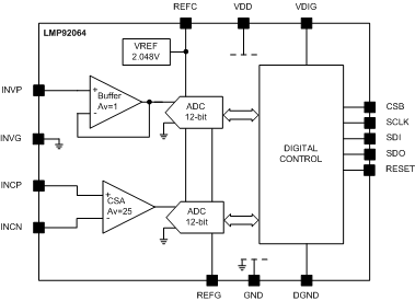
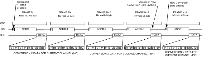 Figure 20. Timing Diagram With Byte Read Frames
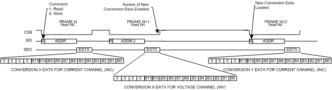 Figure 21. Timing Diagram With Word Read Frames
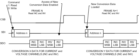 Figure 22. Timing Diagram With All Data Read Frames