SNAS634B March   2014  – January 2016 LMP92066

PRODUCTION DATA.  

  1. Features
  2. Applications
  3. Description
  4. Simplified Schematic
  5. Revision History
  6. Pin Configuration and Functions
  7. Specifications
    1. 7.1 Absolute Maximum Ratings
    2. 7.2 ESD Ratings
    3. 7.3 Recommended Operating Conditions
    4. 7.4 Thermal Information
    5. 7.5 Electrical Characteristics
    6. 7.6 Timing Requirements
    7. 7.7 Output Switching Characteristics
    8. 7.8 Typical Characteristics
  8. Detailed Description
    1. 8.1 Overview
    2. 8.2 Functional Block Diagram
    3. 8.3 Features Description
      1. 8.3.1 Temperature Sensor
      2. 8.3.2 Look-Up-Table (LUT) and Arithmetic-Logic Unit (ALU)
        1. 8.3.2.1 LUT and ALU Organization
        2. 8.3.2.2 LUT Coefficient to Register Mapping
        3. 8.3.2.3 The LUT Input and Output Ranges
      3. 8.3.3 Analog Signal Path
        1. 8.3.3.1 DAC
        2. 8.3.3.2 Buffer Amplifier
        3. 8.3.3.3 Output On and Off Control
      4. 8.3.4 Memory
        1. 8.3.4.1 READ and WRITE Access
        2. 8.3.4.2 Access Control
        3. 8.3.4.3 LUT, NOTEPAD Storage, and EEPROM
      5. 8.3.5 I2C Interface
        1. 8.3.5.1 Supported Data Transfer Formats
        2. 8.3.5.2 Slave Address Selection
    4. 8.4 Device Functional Modes
      1. 8.4.1 Default Operating Mode
      2. 8.4.2 Temperature Sensor Override
      3. 8.4.3 ALU Bypass
      4. 8.4.4 DAC Input Override
      5. 8.4.5 LDMOS and GaN Drives
    5. 8.5 Programming
      1. 8.5.1  Temperature Sensor Output Data Access Registers
      2. 8.5.2  DAC Input Data Registers
      3. 8.5.3  Temperature Sensor Status Register
      4. 8.5.4  Override Control Register
      5. 8.5.5  Override Data Registers
      6. 8.5.6  EEPROM Control Register
      7. 8.5.7  Software RESET Register
      8. 8.5.8  Access Control Register
      9. 8.5.9  Block I2C Access Control Register
      10. 8.5.10 I2C Address LOCK Register
      11. 8.5.11 Output Drive Supply Status Register
      12. 8.5.12 Device Version Register
      13. 8.5.13 EEPROM Burn Counter
      14. 8.5.14 LUT Coefficient Registers
      15. 8.5.15 LUT Control Registers
      16. 8.5.16 Notepad Registers
    6. 8.6 Register Map
  9. Application and Implementation
    1. 9.1 Application Information
    2. 9.2 Typical Applications
      1. 9.2.1 Temperature Compensated Bias Generator for LDMOS Power Amplifer (PA)
        1. 9.2.1.1 Design Requirements
        2. 9.2.1.2 Detailed Design Requirements
        3. 9.2.1.3 Application Curves
      2. 9.2.2 Temperature Compensated Bias Generator for GaN Power Amplifer (PA)
        1. 9.2.2.1 Design Requirements
        2. 9.2.2.2 Detailed Design Procedure
        3. 9.2.2.3 Application Curves
    3. 9.3 Do's and Don'ts
      1. 9.3.1 Output Drive Switching
    4. 9.4 Initialization Setup
      1. 9.4.1 Factory Default
      2. 9.4.2 At Power Up
  10. 10Power Supply Recommendations
    1. 10.1 VDD Supply Sourcing
    2. 10.2 IVDD During EEPROM BURN
    3. 10.3 IVDD During EEPROM TRANSFER
  11. 11Layout
    1. 11.1 Layout Guidelines
    2. 11.2 Layout Example
  12. 12Device and Documentation Support
    1. 12.1 Device Support
      1. 12.1.1 Device Nomenclature
    2. 12.2 Trademarks
    3. 12.3 Electrostatic Discharge Caution
    4. 12.4 Glossary
  13. 13Mechanical, Packaging, and Orderable Information

Package Options

Mechanical Data (Package|Pins)
Thermal pad, mechanical data (Package|Pins)
Orderable Information

11 Layout

11.1 Layout Guidelines

The LMP92066 is a device for which the input signal is temperature. The primary path of heat conduction is through the exposed PowerPAD on the underside of the package. The layout should provide direct, high thermal conductivity path between the LMP92066 and the devices controlled by its output:

  • Use heavy copper layer as the thermal conduction path. This layer must be also a GND node.
  • If the heavy copper layer is not a top layer, use a dense array of vias to connect to both the LMP92066 and the heat sources to maintain high thermal conductivity.
  • Place the LMP92066 in the geometric center between the multiple heat sources in order to minimize the “thermal offsets” due to the temperature gradients.

11.2 Layout Example
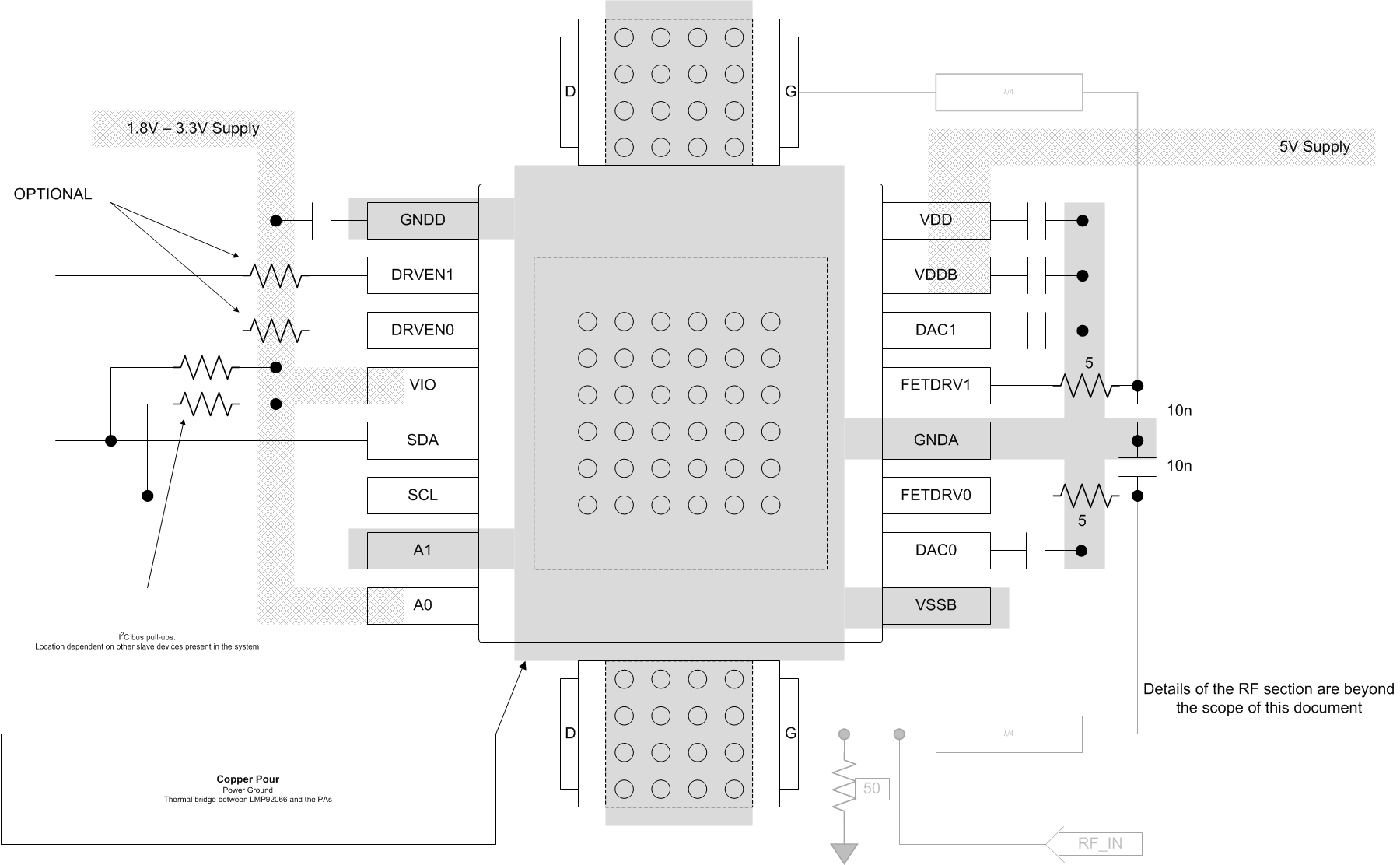
LMP92066 layout_example.gif Figure 53. LMP92066 Layout