SNVS727C October   2011  – June 2019 LMR10510

PRODUCTION DATA.  

  1. Features
  2. Applications
  3. Description
    1.     Device Images
      1.      Simplified Application
  4. Revision History
  5. Description, continued
  6. Pin Configuration and Functions
    1.     Pin Description: 5-Pin SOT-23
    2.     Pin Descriptions 6-Pin WSON
  7. Specifications
    1. 7.1 Absolute Maximum Ratings
    2. 7.2 Recommended Operating Ratings
    3. 7.3 Electrical Characteristics
    4. 7.4 Typical Performance Characteristics
  8. Detailed Description
    1. 8.1 Overview
    2. 8.2 Functional Block Diagram
    3. 8.3 Feature Description
      1. 8.3.1 Soft Start
      2. 8.3.2 Output Overvoltage Protection
      3. 8.3.3 Undervoltage Lockout
      4. 8.3.4 Current Limit
      5. 8.3.5 Thermal Shutdown
  9. Application and Implementation
    1. 9.1 Application Information
    2. 9.2 Typical Application
      1. 9.2.1 Detailed Design Procedure
        1. 9.2.1.1 Custom Design With WEBENCH® Tools
        2. 9.2.1.2 Inductor Selection
        3. 9.2.1.3 Input Capacitor
        4. 9.2.1.4 Output Capacitor
        5. 9.2.1.5 Catch Diode
        6. 9.2.1.6 Output Voltage
        7. 9.2.1.7 Calculating Efficiency, and Junction Temperature
      2. 9.2.2 Application Curves
      3. 9.2.3 Other System Examples
        1. 9.2.3.1 LMR10510x Design Example 1
        2. 9.2.3.2 Lmr10510X Design Example 2
        3. 9.2.3.3 LMR10510Y Design Example 3
        4. 9.2.3.4 LMR10510Y Design Example 4
  10. 10Layout
    1. 10.1 Layout Guidelines
    2. 10.2 Layout Example
    3. 10.3 Thermal Definitions
    4. 10.4 WSON Package
  11. 11Device and Documentation Support
    1. 11.1 Device Support
      1. 11.1.1 Development Support
        1. 11.1.1.1 Custom Design With WEBENCH® Tools
    2. 11.2 Receiving Notification of Documentation Updates
    3. 11.3 Community Resources
    4. 11.4 Trademarks
    5. 11.5 Electrostatic Discharge Caution
    6. 11.6 Glossary
  12. 12Mechanical, Packaging, and Orderable Information

Package Options

Mechanical Data (Package|Pins)
Thermal pad, mechanical data (Package|Pins)
Orderable Information

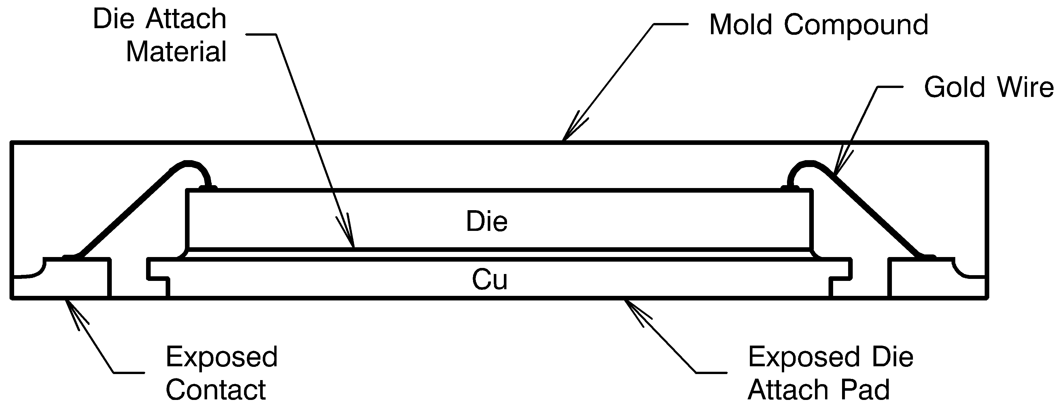
WSON Package

LMR10510 30165668.pngFigure 26. Internal WSON Connection

For certain high power applications, the PCB land may be modified to a "dog bone" shape (see Figure 25). By increasing the size of ground plane, and adding thermal vias, the RθJA for the application can be reduced.