SNVSBD7A October 2019 – February 2020 LMR36510
PRODUCTION DATA.
- 1 Features
- 2 Applications
- 3 Description
- 4 Revision History
- 5 Pin Configuration and Functions
- 6 Specifications
- 7 Detailed Description
- 8 Application and Implementation
- 9 Power Supply Recommendations
- 10Layout
- 11Device and Documentation Support
- 12Mechanical, Packaging, and Orderable Information
Package Options
Mechanical Data (Package|Pins)
- DDA|8
Thermal pad, mechanical data (Package|Pins)
- DDA|8
Orderable Information
7.3.3 Current Limit and Short Circuit
The LMR36510 incorporates valley current limit for normal overloads and for short-circuit protection. In addition, the high-side power MOSFET is protected from excessive current by a peak-current limit circuit. Cycle-by-cycle current limit is used for overloads while hiccup mode is used for short circuits. Finally, a zero current detector is used on the low-side power MOSFET to implement diode emulation at light loads (see the Glossary).
During overloads, the low-side current limit, ILIMIT, determines the maximum load current that the LMR36510 can supply. When the low-side switch turns on, the inductor current begins to ramp down. If the current does not fall below ILIMIT before the next turnon cycle, then that cycle is skipped, and the low-side MOSFET is left on until the current falls below ILIMIT. This is somewhat different than the more typical peak-current limit and results in Equation 1 for the maximum load current.

where
- fSW = switching frequency
- L = inductor value
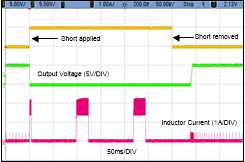
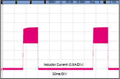
If, during current limit, the voltage on the FB input falls below about 0.4 V due to a short circuit, the device enters into hiccup mode. In this mode, the device stops switching for tHC, or about 94 ms, and then goes through a normal re-start with soft start. If the short-circuit condition remains, the device runs in current limit for about 20 ms (typical) and then shuts down again. This cycle repeats as long as the short-circuit condition persists. This mode of operation reduces the temperature rise of the device during a hard short on the output. Of course, the output current is greatly reduced during hiccup mode. Once the output short is removed and the hiccup delay is passed, the output voltage recovers normally.
The high-side current limit trips when the peak inductor current reaches ISC. This is a cycle-by-cycle current limit and does not produce any frequency or load current foldback. It is meant to protect the high-side MOSFET from excessive current. Under some conditions, such as high input voltages, this current limit can trip before the low-side protection. Under this condition, ISC determines the maximum output current. Note that ISC varies with duty cycle.
 Figure 7. Short-Circuit Transient and Recovery
  Figure 8. Inductor Current Burst in Short Circuit Mode