SNIS189D June 2015 – June 2018 LMT01
PRODUCTION DATA.
- 1 Features
- 2 Applications
- 3 Description
- 4 Revision History
- 5 Pin Configuration and Functions
-
6 Specifications
- 6.1 Absolute Maximum Ratings
- 6.2 ESD Ratings
- 6.3 Recommended Operating Conditions
- 6.4 Thermal Information
- 6.5 Electrical Characteristics
- 6.6 Electrical Characteristics - TO-92/LPG Pulse Count to Temperature LUT
- 6.7 Electrical Characteristics - WSON/DQX Pulse Count to Temperature LUT
- 6.8 Switching Characteristics
- 6.9 Timing Diagram
- 6.10 Typical Characteristics
- 7 Detailed Description
- 8 Application and Implementation
- 9 Power Supply Recommendations
- 10Layout
- 11Device and Documentation Support
- 12Mechanical, Packaging, and Orderable Information
Package Options
Mechanical Data (Package|Pins)
Thermal pad, mechanical data (Package|Pins)
- DQX|2
Orderable Information
8.2.1.2 Detailed Design Procedure
First, select the R and determine the maximum logic low voltage and the minimum logic high voltage while ensuring that when the LMT01 is converting, the minimum (VP – VN) requirement of 2.15 V is met.
- Select R using minimum VP-VN during data transmission (2 V) and maximum output current of the LMT01 (143.75 µA)
- R = (3.0 V – 2 V) / 143.75 µA = 6.993 k the closest 1% resistor is 6.980 k
- 6.993 k is the maximum resistance so if using 1% tolerance resistor the actual resistor value needs to be 1% less than 6.993 k and 6.98 k is 0.2% less than 6.993 k thus 6.81 k must be used.
- Check to see if the 2.15-V minimum voltage during conversion requirement for the LMT01 is met with the maximum IOL of 39 µA and maximum R of 6.81 k + 1%:
- VLMT01 = 3 V – (6.81 k × 1.01) × 39 µA = 2.73 V
- Find the maximum low level voltage range using the maximum R of 6.81 k and maximum IOL of 39 µA:
- VRLmax = (6.81 k × 1.01) × 39 µA = 268 mV
- Find the minimum high level voltage using the minimum R of 6.81 k and minimum IOH of 112.5 µA:
- VRHmin = (6.81 k × 0.99) × 112.5 µA = 758 mV
Now select the MSP430 comparator threshold voltage that enables the LMT01 to communicate to the MSP430 properly.
- The MSP430 voltage is selected by selecting the internal VREF and then choosing the appropriate 1 of n/32 settings for n of 1 to 31.
- VMID= (VRLmax – VRHmin) / 2 + VRHmin = (758 mV – 268 mV) / 2 + 268 mV = 513 mV
- n = (VMID / VREF ) × 32 = (0.513 / 2.5) × 32 = 7
- To prevent oscillation of the comparator, output hysteresis must be implemented. The MSP430 allows this by enabling different n for the rising edge and falling edge of the comparator output. For a falling comparator output transition, N must be set to 6.
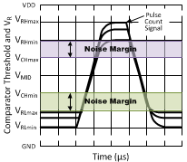
- Determine the noise margin caused by variation in comparator threshold level. Even though the comparator threshold level theoretically is set to VMID, the actual level varies from device to device due to VREF tolerance, resistor divider tolerance, and comparator offset. For proper operation, the COMP_B worst case input threshold levels must be within the minimum high and maximum low voltage levels presented across R, VRHmin and VRLmax, respectively
- VREF is the MSP430 COMP_B reference voltage for this example at 2.5 V
- V_REF_TOL is the tolerance of the VREF of 1% or 0.01,
- N is the divisor for the MSP430 or 7
- N_TOL is the tolerance of the divisor or 0.5
- COMP_OFFSET is the comparator offset specification or 10 mV
- VREF is the MSP430 COMP_B reference voltage for this example at 2.5 V,
- V_REF_TOL is the tolerance of the VREF of 1% or 0.01,
- N is the divisor for the MSP430 for the hysteresis setting or 6,
- N_TOL is the tolerance of the divisor or 0.5,
- COMP_OFFSET is the comparator offset specification or 10 mV
Equation 5.
where
Equation 6.
where
The noise margin is the minimum of the two differences:
Equation 7. (VRHmin – VCHmax) or (VCHmin – VRLmax)which works out to be 145 mV.
 Figure 29. Pulse Count Signal Amplitude Variation