SNIS187A March 2015 – July 2015 LMT70 , LMT70A
PRODUCTION DATA.
- 1 Features
- 2 Applications
- 3 Description
- 4 Wide-Range Precision Active RTD or NTC Replacement (−55°C to 150°C)
- 5 Revision History
- 6 Device Comparison Table
- 7 Pin Configuration and Functions
- 8 Specifications
- 9 Detailed Description
- 10Application and Implementation
- 11Power Supply Recommendations
- 12Layout
- 13Device and Documentation Support
- 14Mechanical, Packaging, and Orderable Information
Package Options
Mechanical Data (Package|Pins)
- YFQ|4
Thermal pad, mechanical data (Package|Pins)
Orderable Information
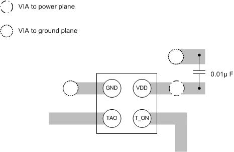
12 Layout
12.1 Layout Guidelines
The LMT70 can be applied easily in the same way as other integrated-circuit temperature sensors. It can be glued or cemented to a surface. The temperatures of the lands and traces to the other leads of the LMT70 will also affect the temperature reading.
12.1.1 Mounting and Temperature Conductivity
Alternatively, the LMT70 can be mounted inside a sealed-end metal tube, and can then be dipped into a bath or screwed into a threaded hole in a tank. As with any IC, the LMT70 and accompanying wiring and circuits must be kept insulated and dry, to avoid leakage and corrosion. This is especially true if the circuit may operate at cold temperatures where condensation can occur. If moisture creates a short circuit from the TAO output to ground or VDD, the TAO output from the LMT70 will not be correct. Printed-circuit coatings are often used to ensure that moisture cannot corrode the leads or circuit traces.
The LMT70's junction temperature is the actual temperature being measured. The thermal resistance junction-to-ambient (RθJA) is the parameter (from Thermal Information) used to calculate the rise of a device junction temperature due to its power dissipation. Equation 1 is used to calculate the rise in the LMT70's die temperature.

where
- TA is the ambient temperature.
- IQ is the quiescent current.
- IL is the load current on VTEMP.
For example, in an application where TA = 30°C, VDD = 3 V, IDD = 12µA, VTAO = 943.227 mV, and IL = 0 μA, the total temperature rise would be [187°C/W × 3 V × 12 μA] = 0.007°C. To minimize self-heating, the load current on TAO pin should be minimized.
12.2 Layout Example
