SNIS187A March   2015  – July 2015 LMT70 , LMT70A

PRODUCTION DATA.  

  1. Features
  2. Applications
  3. Description
  4. Wide-Range Precision Active RTD or NTC Replacement (−55°C to 150°C)
  5. Revision History
  6. Device Comparison Table
  7. Pin Configuration and Functions
  8. Specifications
    1. 8.1 Absolute Maximum Ratings
    2. 8.2 ESD Ratings
    3. 8.3 Recommended Operating Conditions
    4. 8.4 Thermal Information
    5. 8.5 Electrical Characteristics
    6. 8.6 Electrical Characteristics Temperature Lookup Table (LUT)
    7. 8.7 Switching Characteristics
    8. 8.8 Typical Performance Characteristics
  9. Detailed Description
    1. 9.1 Overview
    2. 9.2 Functional Block Diagram
    3. 9.3 Feature Description
      1. 9.3.1 Temperature Analog Output (TAO)
        1. 9.3.1.1 LMT70 Output Transfer Function
          1. 9.3.1.1.1 First Order Transfer Function
          2. 9.3.1.1.2 Second Order Transfer Function
          3. 9.3.1.1.3 Third Order Transfer Function
        2. 9.3.1.2 LMT70A TAO Matching
        3. 9.3.1.3 TAO Noise Considerations
        4. 9.3.1.4 TAO Capacitive Loads
      2. 9.3.2 TON Digital Input
      3. 9.3.3 Light Sensitivity
    4. 9.4 Device Functional Modes
  10. 10Application and Implementation
    1. 10.1 Application Information
    2. 10.2 Typical Application
      1. 10.2.1 Design Requirements
      2. 10.2.2 Detailed Design Procedure
        1. 10.2.2.1 Temperature Algorithm Selection
        2. 10.2.2.2 ADC Requirements
      3. 10.2.3 Finer Resolution LUT
      4. 10.2.4 Application Curves
    3. 10.3 System Examples
  11. 11Power Supply Recommendations
  12. 12Layout
    1. 12.1 Layout Guidelines
      1. 12.1.1 Mounting and Temperature Conductivity
    2. 12.2 Layout Example
  13. 13Device and Documentation Support
    1. 13.1 Related Links
    2. 13.2 Documentation Support
      1. 13.2.1 Related Documentation
    3. 13.3 Community Resources
    4. 13.4 Trademarks
    5. 13.5 Electrostatic Discharge Caution
    6. 13.6 Glossary
  14. 14Mechanical, Packaging, and Orderable Information

Package Options

Mechanical Data (Package|Pins)
Thermal pad, mechanical data (Package|Pins)
Orderable Information

7 Pin Configuration and Functions

DSBGA or WLCSP
4 Pins YFQ
(Top View)
LMT70 LMT70A 30080501.gif

Pin Functions

PIN TYPE EQUIVALENT CIRCUIT DESCRIPTION
NAME NO.
GND A1 Ground Ground reference for the device
VDD A2 Power Supply voltage
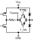
TAO B1 Analog Output LMT70 LMT70A 30080539.gif Temperature analog output pin
T_ON B2 Digital Input LMT70 LMT70A 30080538.gif T_ON pin. Active High input.
If T_ON = 0, then the TAO output is open.
If T_ON = 1, then TAO pin is connected to the temperature output voltage.
Tie this pin to VDD if not used.