SNOS990H April 2002 – June 2016 LMV341-N , LMV342-N , LMV344-N
PRODUCTION DATA.
- 1 Features
- 2 Applications
- 3 Description
- 4 Revision History
- 5 Pin Configuration and Functions
-
6 Specifications
- 6.1 Absolute Maximum Ratings
- 6.2 ESD Ratings
- 6.3 Recommended Operating Conditions
- 6.4 Thermal Information
- 6.5 Electrical Characteristics - 2.7 V (DC)
- 6.6 Electrical Characteristics - 2.7 V (AC)
- 6.7 Electrical Characteristics - 5 V (DC)
- 6.8 Electrical Characteristics - 5 V (AC)
- 6.9 Typical Characteristics
- 7 Detailed Description
- 8 Application and Implementation
- 9 Power Supply Recommendations
- 10Layout
- 11Device and Documentation Support
- 12Mechanical, Packaging, and Orderable Information
Package Options
Mechanical Data (Package|Pins)
Thermal pad, mechanical data (Package|Pins)
Orderable Information
8 Application and Implementation
NOTE
Information in the following applications sections is not part of the TI component specification, and TI does not warrant its accuracy or completeness. TI’s customers are responsible for determining suitability of components for their purposes. Customers should validate and test their design implementation to confirm system functionality.
8.1 Application Information
The LMV34x-N amplifier family features low voltage, low power, rail-to-rail output as well as a shutdown capability, making it well suited for low voltage portable applications.
8.2 Typical Application
8.2.1 Sample and Hold Circuit
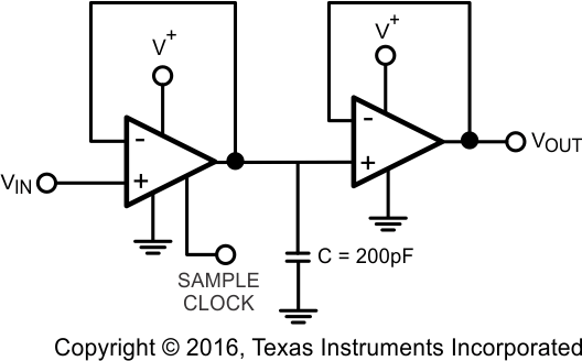
 Figure 46. Sample and Hold Circuit
8.2.1.1 Design Requirements
The lower input bias current of the LMV341-N results in a very high input impedance. The output impedance when the device is in shutdown mode is quite high. These high impedances, along with the ability of the shutdown pin to be derived from a separate power source, make LMV341-N a good choice for sample and hold circuits. The sample clock must be connected to the shutdown pin of the amplifier to rapidly turn the device on or off.
8.2.1.2 Detailed Design Procedure
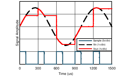
Figure 46 shows the schematic of a simple sample and hold circuit. When the sample clock is high the first amplifier is in normal operation mode and the second amplifier acts as a buffer. The capacitor, which appears as a load on the first amplifier, is charging at this time. The voltage across the capacitor is that of the noninverting input of the first amplifier because it is connected as a voltage-follower. When the sample clock is low the first amplifier is shut off, bringing the output impedance to a high value. The high impedance of this output, along with the very high impedance on the input of the second amplifier, prevents the capacitor from discharging. There is very little voltage droop while the first amplifier is in shutdown mode. The second amplifier, which is still in normal operation mode and is connected as a voltage follower, also provides the voltage sampled on the capacitor at its output.
8.2.1.3 Application Curve
 Figure 47. Sample and Hold Circuit Results