SNOSAQ5H February   2007  – August 2016 LMV551 , LMV552 , LMV554

PRODUCTION DATA.  

  1. Features
  2. Applications
  3. Description
  4. Revision History
  5. Pin Configuration and Functions
  6. Specifications
    1. 6.1 Absolute Maximum Ratings
    2. 6.2 ESD Ratings
    3. 6.3 Recommended Operating Conditions
    4. 6.4 Thermal Information
    5. 6.5 Electrical Characteristics: 3 V
    6. 6.6 Electrical Characteristics: 5 V
    7. 6.7 Typical Characteristics
  7. Detailed Description
    1. 7.1 Overview
    2. 7.2 Functional Block Diagram
    3. 7.3 Feature Description
      1. 7.3.1 Low Voltage and Low Power Operation
      2. 7.3.2 Wide Bandwidth
      3. 7.3.3 Low Input Referred Noise
      4. 7.3.4 Ground Sensing and Rail-to-Rail Output
      5. 7.3.5 Small Size
    4. 7.4 Device Functional Modes
      1. 7.4.1 Stability Of Op Amp Circuits
        1. 7.4.1.1 Stability and Capacitive Loading
          1. 7.4.1.1.1 In the Loop Compensation
          2. 7.4.1.1.2 Compensation by External Resistor
  8. Application and Implementation
    1. 8.1 Application Information
    2. 8.2 Typical Application
      1. 8.2.1 Design Requirements
      2. 8.2.2 Detailed Design Procedure
      3. 8.2.3 Application Curve
    3. 8.3 Do's and Don'ts
  9. Power Supply Recommendations
  10. 10Layout
    1. 10.1 Layout Guidelines
    2. 10.2 Layout Example
  11. 11Device and Documentation Support
    1. 11.1 Device Support
      1. 11.1.1 Development Support
    2. 11.2 Documentation Support
      1. 11.2.1 Related Documentation
    3. 11.3 Related Links
    4. 11.4 Receiving Notification of Documentation Updates
    5. 11.5 Community Resource
    6. 11.6 Trademarks
    7. 11.7 Electrostatic Discharge Caution
    8. 11.8 Glossary
  12. 12Mechanical, Packaging, and Orderable Information

Package Options

Mechanical Data (Package|Pins)
Thermal pad, mechanical data (Package|Pins)
Orderable Information

10 Layout

10.1 Layout Guidelines

The V+ pin should be bypassed to ground with a low-ESR capacitor.

The optimum placement is closest to the V+ and ground pins.

Take care to minimize the loop area formed by the bypass capacitor connection between V+ and ground.

The ground pin should be connected to the PCB ground plane at the pin of the device.

The feedback components should be placed as close to the device as possible minimizing strays.

10.2 Layout Example
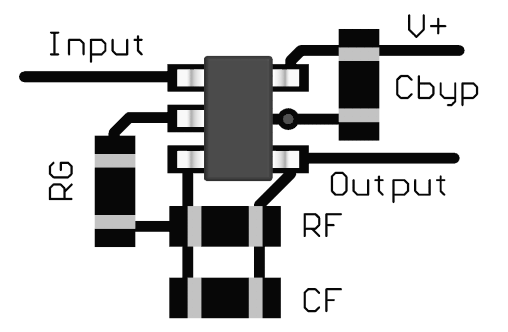
LMV551 LMV552 LMV554 Southwest_Pinout.gif Figure 32. SOT-23 Layout Example