SNOSAI7K September 2005 – May 2016 LMV651 , LMV652 , LMV654
PRODUCTION DATA.
- 1 Features
- 2 Applications
- 3 Description
- 4 Revision History
- 5 Pin Configuration and Functions
- 6 Specifications
- 7 Detailed Description
- 8 Application and Implementation
- 9 Power Supply Recommendations
- 10Layout
- 11Device and Documentation Support
- 12Mechanical, Packaging, and Orderable Information
Package Options
Mechanical Data (Package|Pins)
- PW|14
Thermal pad, mechanical data (Package|Pins)
- PW|14
Orderable Information
7 Detailed Description
7.1 Overview
TI’s LMV65x devices have 12 MHz of bandwidth, are unity-gain stable, and consume only 116 μA of current. They also have a maximum input offset voltage of 1.5 mV, a rail-to-rail output stage, and an input common-mode voltage range that includes ground. Lastly, these operational amplifiers provide a PSRR of 95 dB, a CMRR of 100 dB, and a total harmonic distortion (THD) of 0.003% at 1-kHz frequency and 2-kΩ load.
7.2 Functional Block Diagram

7.3 Feature Description
7.3.1 Low Voltage and Low Power Operation
The LMV65x have performance specified at supply voltages of 3 V and 5 V. These parts are specified to be operational at all supply voltages between 2.7 V and 5.5 V. The LMV651 draws a low supply current of 116 μA, the LMV652 draws 118 μA/channel and the LMV654 draws 122 μA/channel. This family of operational amplifiers provides the low voltage and low power amplification that is essential for portable applications.
7.3.2 Wide Bandwidth
Despite drawing the very low supply current of 116 µA, the LMV65x manage to provide a wide unity-gain bandwidth of 12 MHz. This is easily one of the best bandwidth to power ratios ever achieved, and allows these operational amplifiers to provide wideband amplification while using the minimum amount of power. This makes this family of parts ideal for low-power signal processing applications such as portable media players and other accessories.
7.3.3 Low Input Referred Noise
The LMV65x provides a flatband input referred voltage noise density of 17 nV/√Hz, which is significantly better than the noise performance expected from a low-power operational amplifiers. These operational amplifiers also feature exceptionally low 1/f noise, with a very low 1/f noise corner frequency of 4 Hz. This makes these parts ideal for low power applications which require decent noise performance, such as PDAs and portable sensors.
7.3.4 Ground Sensing and Rail-to-Rail Output
The LMV65x each have a rail-to-rail output stage, which provides the maximum possible output dynamic range. This is especially important for applications requiring a large output swing. The input common-mode range of this family of devices includes the negative supply rail which allows direct sensing at ground in a single-supply operation.
7.3.5 Small Size
The small footprint of the packages for the LMV65x saves space on printed-circuit boards, and enables the design of smaller and more compact electronic products. Long traces between the signal source and the operational amplifier make the signal path susceptible to noise. By using a physically smaller package, these operational amplifiers can be placed closer to the signal source, reducing noise pickup and enhancing signal integrity.
7.4 Device Functional Modes
7.4.1 Stability and Capacitive Loading
If the phase margin of the LMV65x is plotted with respect to the capacitive load (CL) at its output, it is seen that the phase margin reduces significantly if CL is increased beyond 100 pF. This is because the operational amplifier is designed to provide the maximum bandwidth possible for a low supply current. Stabilizing it for higher capacitive loads would have required either a drastic increase in supply current, or a large internal compensation capacitance, which would have reduced the bandwidth of the operational amplifier. Hence, if these devices are to be used for driving higher capacitive loads, they would have to be externally compensated.
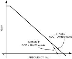
 Figure 34. Gain vs Frequency for an Operational Amplifiers
An operational amplifier, ideally, has a dominant pole close to DC, which causes its gain to decay at the rate of 20 dB/decade with respect to frequency. If this rate of decay, also known as the rate of closure (ROC), remains the same until the unity-gain bandwidth of the operational amplifiers is stable. If, however, a large capacitance is added to the output of the operational amplifier, it combines with the output impedance of the operational amplifier to create another pole in its frequency response before its unity-gain frequency (see Figure 34). This increases the ROC to 40 dB/decade and causes instability.
In such a case a number of techniques can be used to restore stability to the circuit. The idea behind all these schemes is to modify the frequency response such that it can be restored to an ROC of 20 dB/decade, which ensures stability.
7.4.2 In The Loop Compensation
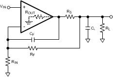
Figure 35 illustrates a compensation technique, known as in-the-loop compensation, that employs an RC feedback circuit within the feedback loop to stabilize a noninverting amplifier configuration. A small series resistance, RS, is used to isolate the amplifier output from the load capacitance, CL, and a small capacitance, CF, is inserted across the feedback resistor to bypass CL at higher frequencies.
 Figure 35. In-the-Loop Compensation
The values for RS and CF are decided by ensuring that the zero attributed to CF lies at the same frequency as the pole attributed to CL. This ensures that the effect of the second pole on the transfer function is compensated for by the presence of the zero, and that the ROC is maintained at 20 dB/decade. For the circuit shown in Figure 35 the values of RS and CF are given by Equation 1. Values of RS and CF required for maintaining stability for different values of CL, as well as the phase margins obtained, are shown in Table 1. RF and RIN are taken to be 10 kΩ, RL is 2 kΩ, while ROUT is taken as 340 Ω.

Table 1. Loop Compensation Values
| CL (pF) | RS (Ω) | CF (pF) | PHASE MARGIN (°) |
|---|---|---|---|
| 150 | 340 | 15 | 39.4 |
| 200 | 340 | 20 | 34.6 |
| 250 | 340 | 25 | 31.1 |
Although this methodology provides circuit stability for any load capacitance, it does so at the price of bandwidth. The closed-loop bandwidth of the circuit is now limited by RF and CF.
7.4.3 Compensation By External Resistor
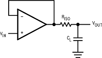
In some applications, it is essential to drive a capacitive load without sacrificing bandwidth. In such a case, in the loop compensation is not viable. A simpler scheme for compensation is shown in Figure 36. A resistor, RISO, is placed in series between the load capacitance and the output. This introduces a zero in the circuit transfer function, which counteracts the effect of the pole formed by the load capacitance, and ensures stability. The value of RISO to be used should be decided depending on the size of CL and the level of performance desired. Values ranging from 5 Ω to 50 Ω are usually sufficient to ensure stability. A larger value of RISO results in a system with lesser ringing and overshoot, but it also limits the output swing and the short-circuit current of the circuit.
 Figure 36. Compensation by Isolation Resistor