SNOS998I February 2002 – October 2015 LMV761 , LMV762 , LMV762Q-Q1
PRODUCTION DATA.
- 1 Features
- 2 Applications
- 3 Description
- 4 Revision History
- 5 Pin Configuration and Functions
-
6 Specifications
- 6.1 Absolute Maximum Ratings
- 6.2 ESD Ratings: LMV761, LMV762
- 6.3 ESD Ratings: LMV762Q-Q1
- 6.4 Recommended Operating Conditions
- 6.5 Thermal Information
- 6.6 2.7-V Electrical Characteristics
- 6.7 5-V Electrical Characteristics
- 6.8 2-V Switching Characteristics
- 6.9 5-V Switching Characteristics
- 6.10 Typical Characteristics
- 7 Detailed Description
- 8 Application and Implementation
- 9 Power Supply Recommendations
- 10Layout
- 11Device and Documentation Support
- 12Mechanical, Packaging, and Orderable Information
Package Options
Mechanical Data (Package|Pins)
Thermal pad, mechanical data (Package|Pins)
- DGK|8
Orderable Information
5 Pin Configuration and Functions
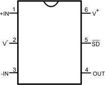
LMV761 (Single) DBV Package
6-Pin SOT-23
Top View

Pin Functions for SOT-23
| PIN | TYPE | DESCRIPTION | |
|---|---|---|---|
| NO. | NAME | ||
| 1 | +IN | I | Noninverting input |
| 2 | V- | P | Negative power terminal |
| 3 | -IN | I | Inverting input |
| 4 | OUT | O | Output |
| 5 | SDB | I | Shutdown (active low) |
| 6 | V+ | P | Positive power terminal |
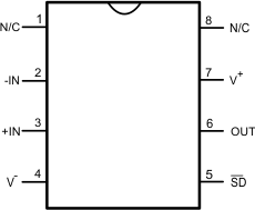
LMV761 (Single) D Package
8-Pin SOIC
Top View

Pin Functions for SOIC (Single)
| PIN | TYPE | DESCRIPTION | |
|---|---|---|---|
| NO. | NAME | ||
| 1 | N/C | — | No Connect (not internally connected) |
| 2 | -IN | I | Inverting Input |
| 3 | +IN | I | Noninverting Input |
| 4 | V- | P | Negative Power Terminal |
| 5 | SDB | I | Shutdown (active low) |
| 6 | OUT | O | Output |
| 7 | V+ | P | Positive Power Terminal |
| 8 | N/C | — | No Connect (not internally connected) |
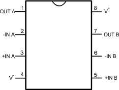
LMV762, LMV762Q-Q1 (Dual) DBV or DGK Package
8-Pin SOIC or VSSOP
Top View

Pin Functions for SOIC and VSSOP (Dual)
| PIN | TYPE | DESCRIPTION | |
|---|---|---|---|
| NO. | NAME | ||
| 1 | OUTA | O | Channel A Output |
| 2 | -INA | I | Channel A Inverting Input |
| 3 | +INA | I | Channel A Noninverting Input |
| 4 | V- | P | Negative Power Terminal |
| 5 | +INB | I | Channel B Noninverting Input |
| 6 | -INB | I | Channel B Inverting Input |
| 7 | OUTB | O | Channel B Output |
| 8 | V+ | P | Positive Power Terminal |