SNOSCP7A March 2013 – January 2016 LMX2485Q-Q1
PRODUCTION DATA.
- 1 Features
- 2 Applications
- 3 Description
- 4 Revision History
- 5 Pin Configuration and Functions
- 6 Specifications
- 7 Parameter Measurement Information
-
8 Detailed Description
- 8.1 Overview
- 8.2 Functional Block Diagram
- 8.3 Feature Description
- 8.4 Device Functional Modes
- 8.5 Programming
- 8.6 Register Maps
- 9 Application and Implementation
- 10Power Supply Recommendations
- 11Layout
- 12Device and Documentation Support
- 13Mechanical, Packaging, and Orderable Information
Package Options
Refer to the PDF data sheet for device specific package drawings
Mechanical Data (Package|Pins)
- RTW|24
Thermal pad, mechanical data (Package|Pins)
- RTW|24
Orderable Information
9 Application and Implementation
NOTE
Information in the following applications sections is not part of the TI component specification, and TI does not warrant its accuracy or completeness. TI’s customers are responsible for determining suitability of components for their purposes. Customers should validate and test their design implementation to confirm system functionality.
9.1 Application Information
This device ideal for use in a broad class of applications, especially those requiring low current consumption and low fractional spurs. For applications that only need a single PLL, the unused PLL can be powered down and will not draw any extra current or generate any spurs or crosstalk. The automotive qualification on this device makes it ideal for automotive applications.
9.2 Typical Application
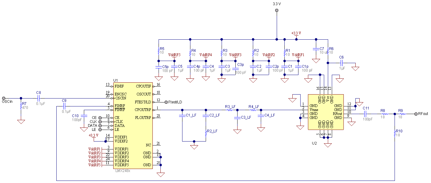
 Figure 33. Typical Application With Only One Side Used
9.2.1 Design Requirements
Table 44 lists the design parameters of the LMX2485Q-Q1.
Table 44. Design Parameters
| PARAMETER | VALUE | |
|---|---|---|
| PM | Phase Margin | 48.3 degrees |
| BW | Loop Bandwidth | 11.3 KHz |
| T3/T1 | Pole Ratio | 40.20% |
| T4/T3 | 36.30% | |
| KPD | Charge Pump Gain | 400 µA |
| fPD | Phase Detector Frequncy | 10 MHz |
| fVCO | VCO Frequency | 2400 – 2480 MHz |
| Vcc | Supply Voltage | 3 V |
| KVCO | VCO Gain | 55 MHz/V |
| CVCO | VCO Input Capacitance | 22 pF |
| C1_LF | Loop Filter Components | 2.7 nF |
| C2_LF | 47 nF | |
| C3_LF | 270 pF | |
| C4_LF | 180 pF | |
| R2_LF | 820 Ω | |
| R3_LF | 3.9 kΩ | |
| R4_LF | 5.6 kΩ | |
9.2.2 Detailed Design Procedure
The design of the loop filter involves balancing requirements of lock time, spurs, and phase noise. This design is fairly involved, but the TI website has references, design tools, and simulation tools cover the loop filter design and simulation in depth.
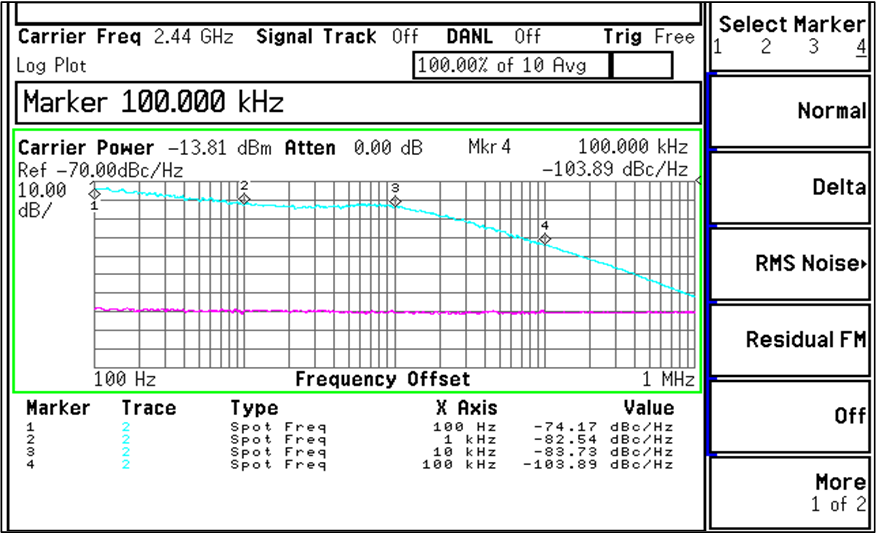
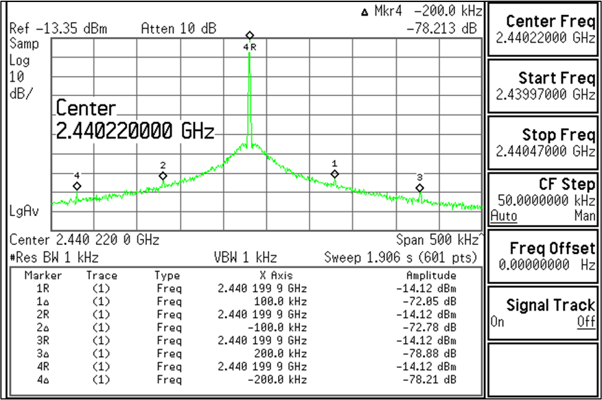
9.2.3 Application Curves

