SNOSCP7A March   2013  – January 2016 LMX2485Q-Q1

PRODUCTION DATA.  

  1. Features
  2. Applications
  3. Description
  4. Revision History
  5. Pin Configuration and Functions
  6. Specifications
    1. 6.1 Absolute Maximum Ratings
    2. 6.2 ESD Ratings - Commercial
    3. 6.3 ESD Ratings - Automotive
    4. 6.4 Recommended Operating Conditions
    5. 6.5 Thermal Information
    6. 6.6 Electrical Characteristics
    7. 6.7 Timing Characteristics
    8. 6.8 Typical Characteristics
      1. 6.8.1 Sensitivity
      2. 6.8.2 FinRF Input Impedance
      3. 6.8.3 FinIF Input Impedance
      4. 6.8.4 OSCin Input Impedance
      5. 6.8.5 Currents
  7. Parameter Measurement Information
    1. 7.1 Bench Test Set-Ups
      1. 7.1.1 Charge Pump Current Measurement Procedure
      2. 7.1.2 Charge Pump Current Specification Definitions
        1. 7.1.2.1 Charge Pump Output Current Variation vs Charge Pump Output Voltage
        2. 7.1.2.2 Charge Pump Sink Current vs Charge Pump Output Source Current Mismatch
        3. 7.1.2.3 Charge Pump Output Current Variation vs Temperature
      3. 7.1.3 Sensitivity Measurement Procedure
      4. 7.1.4 Input Impedance Measurement Procedure
  8. Detailed Description
    1. 8.1 Overview
    2. 8.2 Functional Block Diagram
    3. 8.3 Feature Description
      1. 8.3.1 Tcxo, Oscillator Buffer, and R Counter
      2. 8.3.2 Phase Detector
      3. 8.3.3 Charge Pump
      4. 8.3.4 Loop Filter
      5. 8.3.5 N Counters and High Frequency Input Pins
        1. 8.3.5.1 High Frequency Input Pins, FinRF and FinIF
        2. 8.3.5.2 Complementary High Frequency Pin, FinRF*
      6. 8.3.6 Digital Lock Detect Operation
      7. 8.3.7 Cycle Slip Reduction and Fastlock
        1. 8.3.7.1 Cycle Slip Reduction (CSR)
        2. 8.3.7.2 Fastlock
        3. 8.3.7.3 Using Cycle Slip Reduction (CSR) to Avoid Cycle Slipping
        4. 8.3.7.4 Using Fastlock to Improve Lock Times
        5. 8.3.7.5 Capacitor Dielectric Considerations for Lock Time
      8. 8.3.8 Fractional Spur and Phase Noise Controls
    4. 8.4 Device Functional Modes
      1. 8.4.1 Power Pins, Power Down, and Power Up Modes
    5. 8.5 Programming
      1. 8.5.1 Register Location Truth Table
      2. 8.5.2 Control Register Content Map
    6. 8.6 Register Maps
      1. 8.6.1 R0 Register
      2. 8.6.2 R1 Register
      3. 8.6.3 R2 Register
      4. 8.6.4 R3 Register
      5. 8.6.5 R4 Register
      6. 8.6.6 R5 Register
      7. 8.6.7 R6 Register
      8. 8.6.8 R7 Register
  9. Application and Implementation
    1. 9.1 Application Information
    2. 9.2 Typical Application
      1. 9.2.1 Design Requirements
      2. 9.2.2 Detailed Design Procedure
      3. 9.2.3 Application Curves
  10. 10Power Supply Recommendations
  11. 11Layout
    1. 11.1 Layout Guidelines
    2. 11.2 Layout Example
  12. 12Device and Documentation Support
    1. 12.1 Community Resources
    2. 12.2 Trademarks
    3. 12.3 Electrostatic Discharge Caution
    4. 12.4 Glossary
  13. 13Mechanical, Packaging, and Orderable Information

Package Options

Refer to the PDF data sheet for device specific package drawings

Mechanical Data (Package|Pins)
  • RTW|24
Thermal pad, mechanical data (Package|Pins)
Orderable Information

11 Layout

11.1 Layout Guidelines

The critical pin is the high-frequency input pin that should have a short trace. In general, try to keep the ground and power planes 20 mils or more farther away from vias to supply pins to ensure that no spur energy can couple to them.

11.2 Layout Example
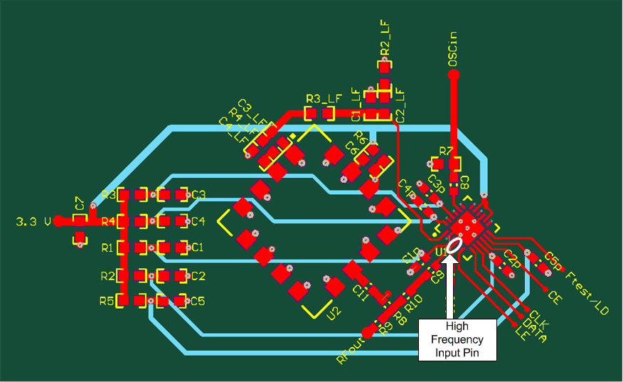
LMX2485Q-Q1 pcb_snoscp7.gif Figure 36. Layout Example