SNOSCP7A March 2013 – January 2016 LMX2485Q-Q1
PRODUCTION DATA.
- 1 Features
- 2 Applications
- 3 Description
- 4 Revision History
- 5 Pin Configuration and Functions
- 6 Specifications
- 7 Parameter Measurement Information
-
8 Detailed Description
- 8.1 Overview
- 8.2 Functional Block Diagram
- 8.3 Feature Description
- 8.4 Device Functional Modes
- 8.5 Programming
- 8.6 Register Maps
- 9 Application and Implementation
- 10Power Supply Recommendations
- 11Layout
- 12Device and Documentation Support
- 13Mechanical, Packaging, and Orderable Information
Package Options
Refer to the PDF data sheet for device specific package drawings
Mechanical Data (Package|Pins)
- RTW|24
Thermal pad, mechanical data (Package|Pins)
- RTW|24
Orderable Information
6 Specifications
6.1 Absolute Maximum Ratings
over operating free-air temperature range (unless otherwise noted)(1)| MIN | MAX | UNIT | ||
|---|---|---|---|---|
| VCC | Power supply voltage | –0.3 | 4.25 | V |
| Vi | Voltage on any pin with GND = 0 V | –0.3 | VCC + 0.3 | V |
| TL | Lead temperature (solder 4 sec.) | 260 | °C | |
| Tstg | Storage temperature | -65 | 150 | °C |
(1) Stresses beyond those listed under Absolute Maximum Ratings may cause permanent damage to the device. These are stress ratings only, which do not imply functional operation of the device at these or any other conditions beyond those indicated under Recommended Operating Conditions. Exposure to absolute-maximum-rated conditions for extended periods may affect device reliability.
6.2 ESD Ratings – Commercial
| VALUE | UNIT | |||
|---|---|---|---|---|
| V(ESD) | Electrostatic discharge(1) | Human-body model (HBM) | ±2000 | V |
| Charged-device model (CDM) | ±750 | |||
| Machine model (MM) | ±200 | |||
(1) This is a high performance RF device is ESD-sensitive. Handling and assembly of this device should be done at an ESD free workstation.
6.3 ESD Ratings – Automotive
| VALUE | UNIT | |||
|---|---|---|---|---|
| V(ESD) | Electrostatic discharge | Human-body model (HBM), per AEC Q100-002(1) | ±2000 | V |
| Charged-device model (CDM), per AEC Q100-011 | ±750 | |||
| ±200 | ||||
(1) AEC Q100-002 indicates that HBM stressing shall be in accordance with the ANSI/ESDA/JEDEC JS-001 specification.
6.4 Recommended Operating Conditions
over operating free-air temperature range (unless otherwise noted)| MIN | NOM | MAX | UNIT | ||
|---|---|---|---|---|---|
| VCC | Power supply voltage(1) | 2.5 | 3 | 3.6 | V |
| TA | Operating temperature | –40 | 25 | 105 | °C |
(1) Absolute Maximum Ratings indicate limits beyond which damage to the device may occur. Recommended Operating Conditions indicate conditions for which the device is intended to be functional, but do not ensure specific performance limits. For ensured specifications and test conditions, see the Electrical Characteristics. The ensured specifications apply only for the test conditions listed. The voltage at all the power supply pins of VddRF1, VddRF2, VddRF3, VddRF4, VddRF5, VddIF1 and VddIF2 must be the same. VCC will be used to refer to the voltage at these pins and ICC will be used to refer to the sum of all currents through all these power pins.
6.5 Thermal Information
| THERMAL METRIC(1) | LMX2485Q-Q1 | UNIT | |
|---|---|---|---|
| RTW (WQFN) | |||
| 24 PINS | |||
| RθJA | Junction-to-ambient thermal resistance | 47.2 | °C/W |
| RθJC(top) | Junction-to-case (top) thermal resistance | 43 | °C/W |
| RθJB | Junction-to-board thermal resistance | 24 | °C/W |
| ψJT | Junction-to-top characterization parameter | 0.8 | °C/W |
| ψJB | Junction-to-board characterization parameter | 24 | °C/W |
| RθJC(bot) | Junction-to-case (bottom) thermal resistance | 7 | °C/W |
(1) For more information about traditional and new thermal metrics, see the Semiconductor and IC Package Thermal Metrics application report, SPRA953.
6.6 Electrical Characteristics
over operating free-air temperature range (unless otherwise noted). (VCC = 3V; -40°C ≤ TA ≤ +105°C unless otherwise specified).| PARAMETER | TEST CONDITIONS | MIN | TYP | MAX | UNIT | ||
|---|---|---|---|---|---|---|---|
| Icc PARAMETERS | |||||||
| ICCRF | Power supply current, RF synthesizer | IF PLL OFF RF PLL ON Charge Pump TRI-STATE |
3.3 | mA | |||
| ICCIF | Power supply current, IF synthesizer | IF PLL ON RF PLL OFF Charge Pump TRI-STATE |
1.7 | mA | |||
| ICCTOTAL | Power supply current, entire synthesizer | IF PLL ON RF PLL ON Charge Pump TRI-STATE |
5 | mA | |||
| ICCPD | Power-down current | CE = ENOSC = 0V CLK, DATA, LE = 0V |
1 | 10 | µA | ||
| RF SYNTHESIZER PARAMETERS | |||||||
| fFinRF | Operating frequency(1) | RF_P = 8 | 500 | 2000 | MHz | ||
| RF_P = 16 | 500 | 3100 | |||||
| pFinRF | Input sensitivity | -15 | 0 | dBm | |||
| fPD | Phase detector frequency(2) | 50 | MHz | ||||
| ICPoutRFSRCE | RF charge pump source current(3) | RF_CPG = 0 VCPoutRF = VCC/2 |
95 | µA | |||
| RF_CPG = 1 VCPoutRF = VCC/2 |
190 | ||||||
| ... | ... | ||||||
| RF_CPG = 15 VCPoutRF = VCC/2 |
1520 | ||||||
| ICPoutRFSINK | RF charge pump sink current(3) | RF_CPG = 0 VCPoutRF = VCC/2 |
–95 | µA | |||
| RF_CPG = 1 VCPoutRF = VCC/2 |
–190 | ||||||
| ... | ... | ||||||
| RF_CPG = 15 VCPoutRF = VCC/2 |
–1520 | ||||||
| ICPoutRFTRI | RF charge pump TRI-STATE current magnitude | 0.5 ≤ VCPoutRF ≤ VCC – 0.5 | 2 | 10 | nA | ||
| | ICPoutRF%MIS | | Magnitude of RF CP sink vs CP source mismatch | VCPoutRF = VCC/2 TA = 25°C |
RF_CPG > 2 | 3% | 10% | ||
| RF_CPG ≤ 2 | 3% | 13% | |||||
| | ICPoutRF%T | | Magnitude of RF CP current vs temperature | VCPoutRF = VCC/2 | 4% | ||||
| IF SYNTHESIZER PARAMETERS | |||||||
| fFinIF | Operating Frequency | 75 | 800 | MHz | |||
| pFinIF | IF Input Sensitivity | -10 | 5 | dBm | |||
| fCOMP | Phase Detector Frequency | 10 | MHz | ||||
| ICPoutIFSRCE | IF Charge Pump Source Current | VCPoutIF = VCC/2 | 3.5 | mA | |||
| ICPoutIFSINK | IF Charge Pump Sink Current | VCPoutIF = VCC/2 | –3.5 | mA | |||
| ICPoutIFTRI | IF Charge Pump TRI-STATE Current Magnitude | 0.5 ≤ VCPoutIF ≤ VCC RF -0.5 | 2 | 10 | nA | ||
| | ICPoutIF%MIS | | Magnitude of IF CP sink vs CP source mismatch | VCPoutIF = VCC/2 TA = 25°C |
1% | 8% | |||
| | ICPoutIF%V | | Magnitude of IF CP Current vs. CP Voltage | 0.5 ≤ VCPoutIF ≤ VCC -0.5 TA = 25°C |
4% | 10% | |||
| | ICPoutIF%TEMP | Magnitude of IF CP current vs temperature | VCPoutIF = VCC/2 | 4% | ||||
| OSCILLATOR PARAMETERS | |||||||
| fOSCin | Oscillator operating frequency | OSC2X = 0 | 5 | 110 | MHz | ||
| OSC2X = 1 | 5 | 20 | MHz | ||||
| vOSCin | Oscillator input sensitivity | 0.5 | VCC | VP-P | |||
| IOSCin | Oscillator input current | –100 | 100 | µA | |||
| SPURS | |||||||
| Spurs in band | See (4) | –55 | dBc | ||||
| PHASE NOISE | |||||||
| LF1HzRF | RF synthesizer normalized phase noise contribution(5) | RF_CPG = 0 | –202 | dBc/Hz | |||
| RF_CPG = 1 | –202 | ||||||
| RF_CPG = 3 | –206 | ||||||
| RF_CPG = 7 | –208 | ||||||
| RF_CPG = 15 | –210 | ||||||
| LF1HzIF | IF synthesizer normalized phase noise contribution | –209 | dBc/Hz | ||||
| DIGITAL INTERFACE (DATA, CLK, LE, ENOSC, CE, Ftest/LD, FLoutRF) | |||||||
| VIH | High-level input voltage | 1.6 | VCC | V | |||
| VIL | Low-level input voltage | 0.4 | V | ||||
| IIH | High-level input current | VIH = VCC | –5 | 5 | µA | ||
| IIL | Low-level input current | VIL = 0 V | –5 | 5 | µA | ||
| VOH | High-level output voltage | IOH = –500 µA | VCC – 0.4 | V | |||
| VOL | Low-level output voltage | IOL = 500 µA | 0.4 | V | |||
(1) A slew rate of at least 100 V/uS is recommended for frequencies below 500 MHz for optimal performance.
(2) For Phase Detector Frequencies above 20 MHz, Cycle Slip Reduction (CSR) may be required. Legal divide ratios are also required.
(3) Refer to table in Table 25 for complete listing of charge pump currents.
(4) In order to measure the in-band spur, the fractional word is chosen such that when reduced to lowest terms, the fractional numerator is one. The spur offset frequency is chosen to be the comparison frequency divided by the reduced fractional denominator. The loop bandwidth must be sufficiently wide to negate the impact of the loop filter. Measurement conditions are: Spur Offset Frequency = 10 kHz, Loop Bandwidth = 100 kHz, Fraction = 1/2000, Comparison Frequency = 20 MHz, RF_CPG = 7, DITH = 0, and a 4th Order Modulator (FM = 0). These are relatively consistent over tuning range.
(5) Normalized Phase Noise Contribution is defined as: LN(f) = L(f) – 20log(N) – 10log(fCOMP) where L(f) is defined as the single side band phase noise measured at an offset frequency, f, in a 1 Hz Bandwidth. The offset frequency, f, must be chosen sufficiently smaller than the PLL loop bandwidth, yet large enough to avoid substantial phase noise contribution from the reference source. Measurement conditions are: Offset Frequency = 11 kHz, Loop Bandwidth = 100 kHz for RF_CPG = 7, Fraction = 1/2000, Comparison Frequency = 20 MHz, FM = 0, DITH = 0.
6.7 Timing Characteristics
over operating free-air temperature range (unless otherwise noted)| MIN | NOM | MAX | UNIT | |||
|---|---|---|---|---|---|---|
| MICROWIRE INTERFACE TIMING | ||||||
| tCS | Data to Clock Set Up Time | See Figure 1 | 25 | ns | ||
| tCH | Data to Clock Hold Time | See Figure 1 | 8 | ns | ||
| tCWH | Clock Pulse Width High | See Figure 1 | 25 | ns | ||
| tCWL | Clock Pulse Width Low | See Figure 1 | 25 | ns | ||
| tES | Clock to Load Enable Set Up Time | See Figure 1 | 25 | ns | ||
| tEW | Load Enable Pulse Width | See Figure 1 | 25 | ns | ||
 Figure 1. Microwire Input Timing Diagram
6.8 Typical Characteristics
6.8.1 Sensitivity
Typical characteristics do not imply any sort of specification. Ensured specifications are in the Electrical Characteristics section.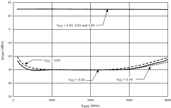
TA = 25°C, RF_P = 16
Figure 2. RF PLL Fin Sensitivity
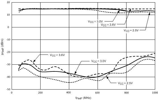
TA = 25°C, IF_P = 16
Figure 4. IF PLL Fin Sensitivity
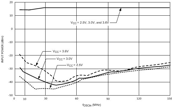
TA = 25°C, OSC_2X = 0
Figure 6. OSCin Sensitivity
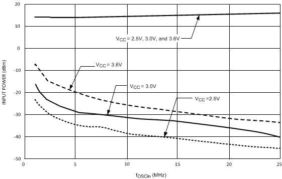
TA = 25°C, OSC_2X = 1
Figure 8. OSCin Sensitivity
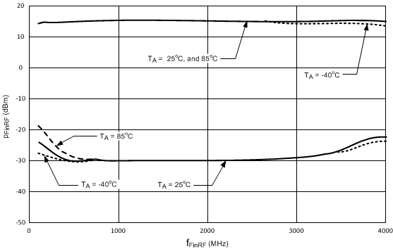
VCC = 3 V, RF_P = 16
Figure 3. RF PLL Fin Sensitivity
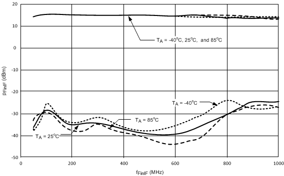
VCC = 3 V, IF_P = 16
Figure 5. IF PLL Fin Sensitivity
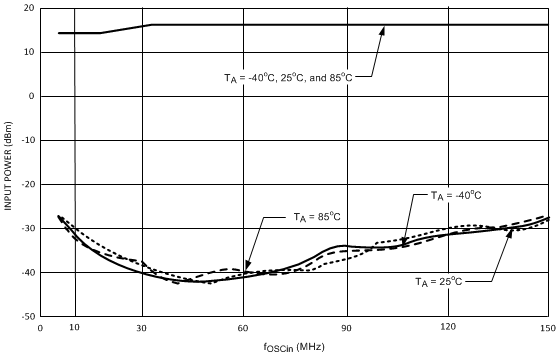
VCC = 3 V, OSC_2X = 0
Figure 7. OSCin Sensitivity
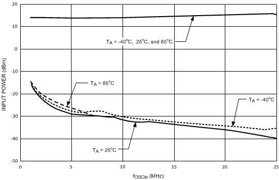
VCC = 3 V, OSC_2X = 1
Figure 9. OSCin Sensitivity
6.8.2 FinRF Input Impedance
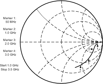 Figure 10. FinRF Input Impedance
Table 1. RF PLL Input Impedance
| FREQUENCY (MHz) | REAL (Ω) | IMAGINARY (Ω) |
|---|---|---|
| 50 | 670 | –276 |
| 100 | 531 | –247 |
| 200 | 452 | –209 |
| 300 | 408 | –212 |
| 400 | 373 | –222 |
| 500 | 337 | –231 |
| 600 | 302 | –237 |
| 700 | 270 | –239 |
| 800 | 241 | –236 |
| 900 | 215 | –231 |
| 1000 | 192 | –221 |
| 1100 | 172 | –218 |
| 1200 | 154 | –209 |
| 1300 | 139 | –200 |
| 1400 | 127 | –192 |
| 1500 | 114 | –184 |
| 1600 | 104 | –175 |
| 1700 | 96 | –168 |
| 1800 | 88 | –160 |
| 1900 | 80 | –153 |
| 2000 | 74 | –147 |
| 2200 | 64 | –134 |
| 2400 | 56 | –123 |
| 2600 | 50 | –113 |
| 2800 | 45 | –103 |
| 3000 | 39 | –94 |
| 3200 | 37 | –86 |
| 3400 | 33 | –78 |
| 3600 | 30 | –72 |
| 3800 | 28 | –69 |
| 4000 | 26 | –66 |
6.8.3 FinIF Input Impedance
Typical characteristics do not imply any sort of specification. Ensured specifications are in the Electrical Characteristics section.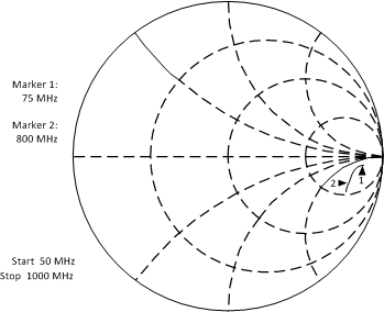 Figure 11. FinIF Input Impedance
Table 2. IF PLL Input Impedance
| FinIF INPUT IMPEDANCE | ||
|---|---|---|
| FREQUENCY (MHz) | REAL (Ω) | IMAGINARY (Ω) |
| 50 | 583 | –286 |
| 75 | 530 | –256 |
| 100 | 499 | –241 |
| 200 | 426 | –209 |
| 300 | 384 | –209 |
| 400 | 347 | –219 |
| 500 | 310 | –224 |
| 600 | 276 | –228 |
| 700 | 244 | –228 |
| 800 | 216 | –223 |
| 900 | 192 | –218 |
| 1000 | 173 | –208 |
6.8.4 OSCin Input Impedance
Typical characteristics do not imply any sort of specification. Ensured specifications are in the Electrical Characteristics section.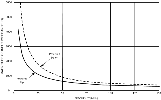 Figure 12. OSCin Input Impedance Magnitude
Table 3. OSCin Input Impedance
| FREQUENCY (MHz) | POWERED-UP | POWERED-DOWN | ||||
|---|---|---|---|---|---|---|
| REAL | IMAGINARY | MAGNITUDE | REAL | IMAGINARY | MAGNITUDE | |
| 5 | 1730 | –3779 | 4157 | 392 | –8137 | 8146 |
| 10 | 846 | –2236 | 2391 | 155 | –4487 | 4490 |
| 20 | 466 | –1196 | 1284 | 107 | –2215 | 2217 |
| 30 | 351 | –863 | 932 | 166 | –1495 | –1504 |
| 40 | 316 | –672 | 742 | 182 | –1144 | 1158 |
| 50 | 278 | –566 | 631 | 155 | –912 | 925 |
| 60 | 261 | –481 | 547 | 153 | –758 | 774 |
| 70 | 252 | –425 | 494 | 154 | –652 | 669 |
| 80 | 239 | –388 | 456 | 147 | –576 | 595 |
| 90 | 234 | –358 | 428 | 145 | –518 | 538 |
| 100 | 230 | –337 | 407 | 140 | –471 | 492 |
| 110 | 225 | –321 | 392 | 138 | –436 | 458 |
| 120 | 219 | –309 | 379 | 133 | –402 | 123 |
| 130 | 214 | –295 | 364 | 133 | –374 | 397 |
| 140 | 208 | –285 | 353 | 132 | –349 | 373 |
| 150 | 207 | –279 | 348 | 133 | –329 | 355 |
6.8.5 Currents
Typical characteristics do not imply any sort of specification. Ensured specifications are in the Electrical Characteristics section.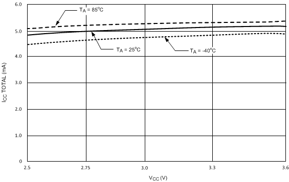
CE = High
Figure 13. Power Supply Current
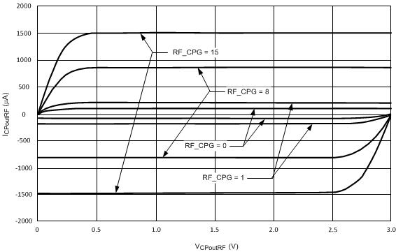
VCC = 3 V
Figure 15. RF PLL Charge Pump Current
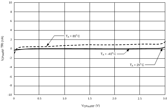
VCC = 3 V
Figure 17. Charge Pump LeakageRF PLL
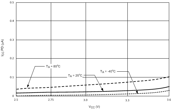
CE = LOW
Figure 14. Power Supply Current
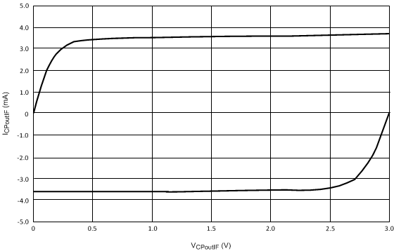
VCC = 3 V
Figure 16. IF PLL Charge Pump Current
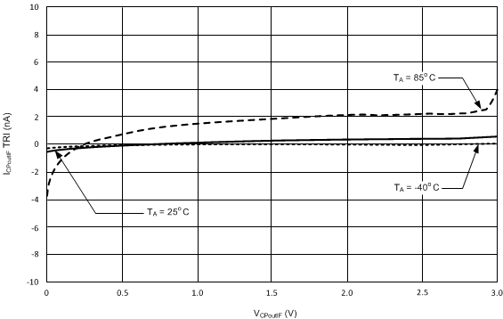
VCC = 3 V
Figure 18. Charge Pump LeakageIF PLL