SNAS654A March 2015 – July 2016 LMX2571
PRODUCTION DATA.
- 1 Features
- 2 Applications
- 3 Description
- 4 Revision History
- 5 Pin Configuration and Functions
- 6 Specifications
-
7 Detailed Description
- 7.1 Overview
- 7.2 Functional Block Diagram
- 7.3
Feature Description
- 7.3.1 Reference Oscillator Input
- 7.3.2 R-Dividers and Multiplier
- 7.3.3 PLL Phase Detector and Charge Pump
- 7.3.4 PLL N-Divider and Fractional Circuitry
- 7.3.5 Partially Integrated Loop Filter
- 7.3.6 Low-Noise, Fully Integrated VCO
- 7.3.7 External VCO Support
- 7.3.8 Programmable RF Output Divider
- 7.3.9 Programmable RF Output Buffer
- 7.3.10 Integrated TX, RX Switch
- 7.3.11 Powerdown
- 7.3.12 Lock Detect
- 7.3.13 FSK Modulation
- 7.3.14 FastLock
- 7.3.15 Register Readback
- 7.4 Device Functional Modes
- 7.5 Programming
- 7.6
Register Maps
- 7.6.1 R60 Register (offset = 3Ch) [reset = 4000h]
- 7.6.2 R58 Register (offset = 3Ah) [reset = C00h]
- 7.6.3 R53 Register (offset = 35h) [reset = 2802h]
- 7.6.4 R47 Register (offset = 2Fh) [reset = 0h]
- 7.6.5 R46 Register (offset = 2Eh) [reset = 1Ah]
- 7.6.6 R42 Register (offset = 2Ah) [reset = 210h]
- 7.6.7 R41 Register (offset = 29h) [reset = 810h]
- 7.6.8 R40 Register (offset = 28h) [reset = 101Ch]
- 7.6.9 R39 Register (offset = 27h) [reset = 11F0h]
- 7.6.10 R35 Register (offset = 23h) [reset = 647h]
- 7.6.11 R34 Register (offset = 22h) [reset = 1000h]
- 7.6.12 R33 Register (offset = 21h) [reset = 0h]
- 7.6.13 R25 to R32 Register (offset = 19h to 20h) [reset = 0h]
- 7.6.14 R24 Register (offset = 18h) [reset = 10h]
- 7.6.15 R23 Register (offset = 17h) [reset = 10A4h]
- 7.6.16 R22 Register (offset = 16h) [reset = 8584h]
- 7.6.17 R21 Register (offset = 15h) [reset = 101h]
- 7.6.18 R20 Register (offset = 14h) [reset = 28h]
- 7.6.19 R19 Register (offset = 13h) [reset = 0h]
- 7.6.20 R18 Register (offset = 12h) [reset = 0h]
- 7.6.21 R17 Register (offset = 11h) [reset = 0h]
- 7.6.22 R9 to R16 Register (offset = 9h to 10h) [reset = 0h]
- 7.6.23 R8 Register (offset = 8h) [reset = 10h]
- 7.6.24 R7 Register (offset = 7h) [reset = 10A4h]
- 7.6.25 R6 Register (offset = 6h) [reset = 8584h]
- 7.6.26 R5 Register (offset = 5h) [reset = 101h]
- 7.6.27 R4 Register (offset = 4h) [reset = 28h]
- 7.6.28 R3 Register (offset = 3h) [reset = 0h]
- 7.6.29 R2 Register (offset = 2h) [reset = 0h]
- 7.6.30 R1 Register (offset = 1h) [reset = 0h]
- 7.6.31 R0 Register (offset = 0h) [reset = 3h]
-
8 Application and Implementation
- 8.1
Application Information
- 8.1.1 Direct Digital FSK Modulation
- 8.1.2 Frequency and Output Port Switching with TrCtl Pin
- 8.1.3 OSCin Configuration
- 8.1.4 Register R0 F1F2_INIT, F1F2_MODE usage
- 8.1.5 FastLock with External VCO
- 8.1.6 OSCin Slew Rate
- 8.1.7 RF Output Buffer Power Control
- 8.1.8 RF Output Buffer Type
- 8.1.9 MULT Multiplier
- 8.1.10 Integrated VCO
- 8.2 Typical Applications
- 8.3 Do's and Don'ts
- 8.1
Application Information
- 9 Power Supply Recommendations
- 10Layout
- 11Device and Documentation Support
- 12Mechanical, Packaging, and Orderable Information
Package Options
Refer to the PDF data sheet for device specific package drawings
Mechanical Data (Package|Pins)
- NJK|36
Thermal pad, mechanical data (Package|Pins)
Orderable Information
8 Application and Implementation
NOTE
Information in the following applications sections is not part of the TI component specification, and TI does not warrant its accuracy or completeness. TI’s customers are responsible for determining suitability of components for their purposes. Customers should validate and test their design implementation to confirm system functionality.
8.1 Application Information
8.1.1 Direct Digital FSK Modulation
In fractional mode, the finest delta frequency difference between two programmable output frequencies is equal to
In other words, when the fractional numerator is incremented by 1 (one step), the output frequency will change by Δfmin. A two steps increment will therefore change the frequency by 2 * Δfmin.
In FSK operation, the instantaneous carrier frequency is kept changing among some pre-defined frequencies. In general, the instantaneous carrier frequency is defined as a certain frequency deviation from the nominal carrier frequency. The frequency deviation could be positive and negative.
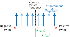 Figure 51. General FSK Definition
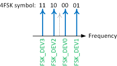 Figure 52. Typical 4FSK Definition
The following equations define the number of steps required for the desired frequency deviation with respect to the nominal carrier frequency output at the RFoutTx or RFoutRx port.
Table 32. FSK Step Equations
| POLARITY | SYNTHESIZER MODE | PLL MODE |
|---|---|---|
| POSITIVE SWING |
Equation 4.
 |
Equation 5.
 |
| NEGATIVE SWING |
Equation 6. 2's complement of Equation 4
|
Equation 7. 2's complement of Equation 5
|
In FSK PIN mode and FSK SPI mdoe, register R25-32 and R9-16 are used to store the desired FSK frequency deviations in term of the number of step as defined in the above equations. The order of the registers, 0 to 7, depends on the application system. A typical 4FSK definition is shown in Figure 52. In this case, FSK_DEV0_Fx and FSK_DEV1_Fx shall be calculated using Equation 4 or Equation 5 while FSK_DEV2_Fx and FSK_DEV3_Fx shall be calculated using Equation 6 or Equation 7.
For example, if FSK PIN mode is enabled in F1 to support 4FSK modulation, set
FSK_MODE_SEL1 = 0
FSK_MODE_SEL0 = 0
FSK_LEVEL = 2
FSK_EN_F1 = 1
Table 33. FSK PIN Mode Example
| RAW FSK DATA STREAM INPUT | EQUIVALENT SYMBOL INPUT | REGISTER SELECTED | RF OUTPUT |
|---|---|---|---|
 |
10 | FSK_DEV2_F1 |  |
| 11 | FSK_DEV3_F1 | ||
| 10 | FSK_DEV2_F1 | ||
| 11 | FSK_DEV3_F1 | ||
| 01 | FSK_DEV1_F1 | ||
| 00 | FSK_DEV0_F1 | ||
| ... | ... |
FSK SPI mode assumes the user knows which symbol to send; user can directly write to register R34, FSK_DEV_SEL to select the desired frequency deviation.
For example, to enable the device to support 4FSK modulation at F1 using FSK SPI mode, set
FSK_MODE_SEL1 = 0
FSK_MODE_SEL0 = 1
FSK_LEVEL = 2
FSK_EN_F1 = 1
Table 34. FSK SPI Mode Example
| DESIRED SYMBOL | WRITE REGISTER FSK_DEV_SEL | REGISTER SELECTED |
|---|---|---|
| 10 | 2 | FSK_DEV2_F1 |
| 11 | 3 | FSK_DEV3_F1 |
| 10 | 2 | FSK_DEV2_F1 |
| 11 | 3 | FSK_DEV3_F1 |
| 01 | 1 | FSK_DEV1_F1 |
| 00 | 0 | FSK_DEV0_F1 |
| ... | ... | … |
Both the FSK PIN mode and FSK SPI mode support up to 8 levels of FSK. To support an arbitrary-level FSK, use FSK SPI FAST mode or FSK I2S mode. Constructing pulse-shaping FSK modulation by over-sampling the FSK modulation waveform is one of the use cases of these modes.
Analog-FM modulation can also be produced in these modes. For example, with a 1-kHz sine wave modulation signal with peak frequency deviation of ±2 kHz, the signal can be over-sampled, say 10 times. Each sample point corresponding to a scaled frequency deviation.
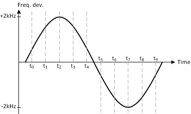 Figure 53. Over-Sampling Modulation Signal
In FSK SPI FAST mode, write the desired FSK steps directly to register R33, FSK_DEV_SPI_FAST. To enable this mode, set
FSK_MODE_SEL1 = 1
FSK_MODE_SEL0 = 1
FSK_EN_F1 = 1
Table 35. FSK SPI FAST Mode Example
| TIME | FREQUENCY DEVIATION | CORRESPONDING FSK STEPS(1) | BINARY EQUIVALENT | WRITE TO FSK_DEV_SPI_FAST |
|---|---|---|---|---|
| t0 | 618.034 Hz | 518 | 0000 0010 0000 0110 | 518 |
| t1 | 1618.034 Hz | 1357 | 0000 0101 0100 1101 | 1357 |
| t2 | 2000 Hz | 1678 | 0000 0110 1000 1110 | 1678 |
| … | … | … | … | … |
| t6 | –1618.034 Hz | 64178 | 1111 1010 1011 0010 | 64178 |
| t7 | –2000 Hz | 63857 | 1111 1001 0111 0001 | 63857 |
| … | … | … | … | … |
In FSK I2S mode, clock in the desired binary format FSK steps in the FSK_D1 pin.
 Figure 54. FSK I2S Mode Example
To enable FSK I2S mode, set
FSK_MODE_SEL1 = 1
FSK_MODE_SEL0 = 0
FSK_EN_F1 =1
8.1.2 Frequency and Output Port Switching with TrCtl Pin
Register R0, RXTX_CTRL, and RXTX_POL are used to define the output port switching behavior with the TrCtl pin. To enable switching with TrCtl pin, set RXTX_CTRL=1.
Table 36. TrCtl Pin Usage
| RXTX_CTRL | RXTX_POL | TrCtl PIN | RFoutTx | RFoutRx |
|---|---|---|---|---|
| 1 | 0 | 0 | Active | |
| 1 | 0 | 1 | Active | |
| 1 | 1 | 0 | Active | |
| 1 | 1 | 1 | Active |
Register R0, F1F2_CTRL, and F1F2_SEL define the operation of the frequency switching between the two pre-defined frequencies F1 and F2. To switch frequency using the TrCtl pin, set F1F2_CTRL to 1. F1F2_SEL selects the output frequency for the current status. For example, if the current active output frequency is F1, toggling TrCtl pin will change the output frequency to F2. Toggling TrCtl pin again will change the output frequency back to F1.
8.1.3 OSCin Configuration
OSCin supports single-end clock, differential clock as well as crystal. Register R34 defines OSCin configuration.
Table 37. OSCin Configuration
| OSCin TYPE | SINGLE-ENDED CLOCK | DIFFERENTIAL CLOCK | CRYSTAL |
|---|---|---|---|
| Connection Diagram |  |
 |
 |
| Register Setting | IPBUF_SE_DIFF_SEL = 0 | IPBUF_SE_DIFF_SEL = 1 IPBUFDIFF_TERM = 1 |
XTAL_EN = 1 XTAL_PWRCTRL = Crystal dependent |
Single-ended and differential input clock definitions are as follows:
 Figure 55. Input Clock Definition
The integrated crystal-oscillator circuit supports a fundamental mode, AT-cute crystal. The load capacitance, CL, is specific to the crystal, but usually on the order of 18 to 20 pF. While CL is specified for crystal, the OSCin input capacitance, CIN (1 pF typical), of the device and PCB stray capacitance, CSTRAY (approximately 1 to 3 pF), can affect the discrete load capacitor values, C1 and C2.
For the parallel resonant circuit, the discrete capacitor values can be calculated as follows:
Typically, C1 = C2 for optimum symmetry, so Equation 8 can be rewritten in terms of C1 only:
Finally, solve for C1:
Electrical Characteristics provide crystal interface specifications with conditions that ensure start-up of the crystal, but it does not specify crystal power dissipation. The designer will need to ensure the crystal power dissipation does not exceed the maximum drive level specified by the crystal manufacturer. Over-driving the crystal can cause premature aging, frequency shift, and eventual failure. Drive level should be held at a sufficient level necessary to start-up and maintain steady-state operation. The power dissipated in the crystal, PXTAL, can be computed by:
where
- IRMS is the rms current through the crystal
- RESR is the maximum equivalent series resistance specified for the crystal
- CL is the load capacitance specified for the crystal
- Co is the minimum shunt capacitance specified for the crystal
- IRMS can be measured using a current probe (for example, Tektronix CT-6 or equivalent) placed on the leg of the crystal connected to OSCin pin with the oscillation circuit active.
The internal configurable resistor, Rd, can be used to limit the crystal drive level, if necessary. If the power dissipated in the selected crystal is higher than the drive level specified for the crystal with Rd shorted, then a larger resistor value is mandatory to avoid over-driving the crystal. However, if the power dissipated in the crystal is less than the drive level with Rd shorted, then a zero value for Rd can be used. As a starting point, a suggested value for Rd is 200 Ω.
8.1.4 Register R0 F1F2_INIT, F1F2_MODE usage
These register bits are used to define the calibration behavior. Correct setting is important to ensure that every F1-F2 switching time is optimized. Figure 56 illustrates the usage of these register bits.
 Figure 56. F1F2_INIT, F1F2_MODE Usage
Before t0: Device initialization
- Power up the device.
- Write all registers to the device.
- Ensure FCAL_EN = 1 to enable calibration.
- Set F1F2_MODE = 1 to make both F1 and F2 being calibrated during initialization. If F1F2_MODE = 0, only the output frequency (F1 in this example) will be calibrated, F2 will not be calibrated. Furthermore, if F1F2 switching is triggered by the TrCtl pin, F1F2_MODE must be equal to 1.
- Set F1F2_INIT = 0. Although the setting of this bit is irrelevant and not important here but if F1F2_INIT = 1, change it back to zero before attempting to change the frequency from F1 to F2.
At t0: Locked to F1
After initialization, both F1 and F2 are calibrated. The calibration data is stored in the internal memory.
At t1: Switch to F2.
Since FCAL_EN = 1, calibration will start over again when the output is switching from F1 to F2. F2 calibration begins based on the last calibration data, which is the calibration data obtained at t0. If the environment (for example, temperature) does not change much, the new calibration data will be similar to the old data. As a result, the calibration time is minimal and therefore, the switching time will be short.
At t2: Switch back to F1
Again, F1 calibration starts over and begins with the last calibration data as obtained at t0. Calibration time is again very short, as is the switching time.
At t3: Switch again to F2
This time, the calibration begins with the calibration data obtained at t1, which is the last calibration data.
At t4: Switch back to F1
Calibration begins with the calibration data obtained at t2, which is the last calibration data.
At t5: Set new F1, F2 frequency
- Write to the relevant registers to set the new F1 and F2 frequency (for example, change the N-divider values)
- Initiate calibration by re-writing register R0
- Set F1F2_INIT=1. Both F1' and F2' will be calibrated
At t6: Locked to F1'
F1' and F2' calibration completed and their calibration data are ready.
At t7: Release F1F2_INIT bit
This bit has to be reset to zero or otherwise both F1' and F2' will be calibrated every time they are toggling.
At t8: F1' calibration data is updated
Since F1F2_INIT is located in register R0, when writing F1F2_INIT = 0 to the device, calibration is once again triggered. However, only F1' will be re-calibrated, the calibration data of F2' remains unchanged.
At t9: Switch to F2'
F2' calibration begins with the calibration data obtained at t6, which is the last calibration data. Calibration time is again very short, as is the switching time.
At t10: Switch back to F1'
F1' calibration starts over and begins with the last calibration data as obtained at t8.
At t11: Switch again to F2'
The calibration begins with the calibration data obtained at t9, which is the last calibration data.
As illustrated above, register F1F2_INIT must be used properly in order to ensure that every F1-F2 switching time is optimized.
8.1.5 FastLock with External VCO
Fastlock may be required in PLL mode where an external VCO with a narrow loop bandwidth is desired. The LMX2571 adopts a new FastLock approach to support the very fast switching time requirement in PLL mode.
There are two control pins in the chip, FLout1 and FLout2. Each pin is used to control a SPST analog switch, S1 and S2. The loop filter value with or without FastLock is the same, except that with FastLock, one more C2 and two SPST switches are needed.
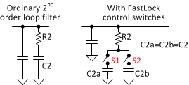 Figure 57. FastLock with SPST Switches
When LMX2571 is locked to F1, FLout1 will close the switch S1. When LMX2571 is locked to F2, either by toggling the TrCtl pin or program register R0, F1F2_SEL, S1 will be released while S2 will be closed by FLout2. Although S1 is released, the charge stored in C2a remains unchanged. Thus, when the output is switched back to F1, the Vtune voltage is almost correct, no (or little) charging or discharging to C2a is required which speeds up the switching time. For example, if Vtune for F1 and F2 are 1 V and 2 V, respectively, without FastLock, when the switching frequency shifts from F1 to F2, C2 will have to be re-charged from 1 V to 2 V — this is a big voltage jump. With FastLock, when S2 is closed, Vtune is almost equal to 2 V because C2b maintains the charge. Only a tiny voltage jump (re-charge) is required to make it reach the final Vtune voltage.
Figure 58 and Figure 59 compare the frequency switching time using different switching methods. In both cases, the loop bandwidth is 4 kHz while fPD is 28 MHz. Figure 58 shows the switching time for a frequency jump from 430 MHz to 480 MHz with SPST switches. Frequency switching is toggled by the TrCtl pin. Switching time is approximately 1 ms. Frequency switching in Figure 59 is done in the traditional way. That is, change the output frequency by writing to the relevant registers such as N-divider values. In this case, because fPD is very much bigger than the loop bandwidth, cycle slipping jeopardizes the switching time to more than 20 ms.
 Figure 58. F1F2 Switching With SPST Switches
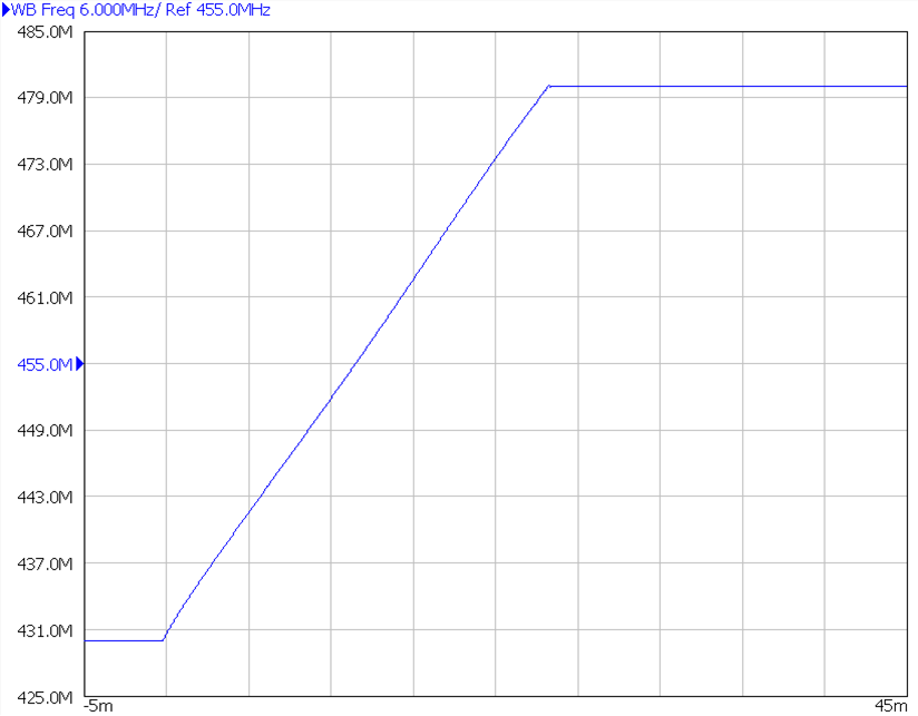 Figure 59. Change F1 Frequency Via SPI Programming
8.1.6 OSCin Slew Rate
A phase-lock loop consists of a clean reference clock, a PLL, and a VCO. Each of these contributes to the total phase noise. The LMX2571 is a high-performance PLL with integrated VCO. Both PLL noise and VCO noise are very good. Typical PLL 1/f noise and noise floor are –124 dBc/Hz and –231 dBc/Hz, respectively. To get the best possible phase-noise performance from the device the quality of the reference clock is very important because it may add noise to the loop. First of all, the phase noise of the reference clock must be good so that the final performance of the system is not degraded. Furthermore, using reference clock with a rather high slew rate (such as a square wave) is highly preferred. Driving the device input with a lower slew rate clock will degrade the device phase noise.
For a given frequency, a sine wave clock has the slowest slew rate, especially when the frequency is low. A CMOS clock or differential clock have much faster slew rates and are recommended. Figure 60 shows a phase-noise comparison with different types of reference clocks. Output frequency is 480 MHz while the input clock frequency is 26 MHz. As one can see there is a 5-dB difference in phase noise when using a clipped sine wave TCXO compared to a differential LVPECL clock. The internal crystal oscillator of the LMX2571 performance is also very good. If temperature compensation is not required, use crystal as the reference clock is a very good price-performance option.
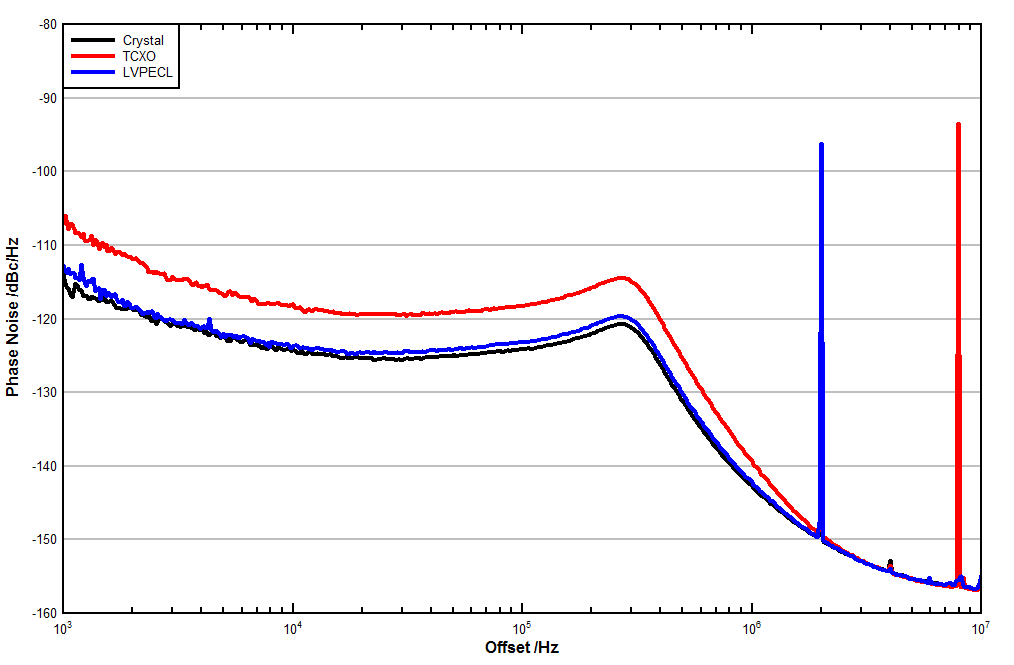 Figure 60. Phase Noise vs Input Clock
8.1.7 RF Output Buffer Power Control
Registers OUTBUF_TX_PWR_Fx and OUTBUF_RX_PWR_Fx are used to set the output power at the RFoutTx and RFoutRx ports. Figure 61 shows a typical output power vs power control bit plot in synthesizer mode. VCO frequency was 4800 MHz, and channel dividers were set to produce the shown output frequencies.
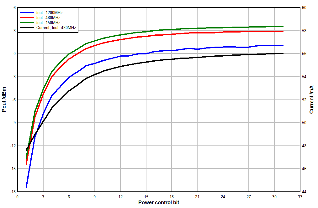 Figure 61. Configurable RF Output Power
8.1.8 RF Output Buffer Type
Registers R35, OUTBUF_TX_TYPE, OUTBUF_RX_TYPE are used to configure the RF output buffer type between open drain and push-pull. Push-pull is easy to use; all that is required is a DC-blocking capacitor at the output. The output waveform is square wave and therefore, harmonics rich. Open-drain output provides an option to reduce the harmonics using an LC resonant pullup network at its output. Table 38 summarizes an example an open-drain vs push-pull application.
Table 38. RF Output Buffer Type
| BUFFER TYPE | OPEN DRAIN | PUSH-PULL | ||||
|---|---|---|---|---|---|---|
| Connection Diagram | 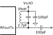 |
 |
||||
| Output Power | 470 MHz | 480 MHz | 490 MHz | 470 MHz | 480 MHz | 490 MHz |
| fo | 2.7 dBm | 2.8 dBm | 2.8 dBm | –0.1 dBm | 0 dBm | 0.1 dBm |
| 2fo | –31 dBc | –30.7 dBc | –30.5 dBc | –30.4 dBc | –30.2 dBc | –30 dBc |
| 3fo | –17.3 dBc | –17.9 dBc | –18.1 dBc | –11.9 dBc | –12.1 dBc | –12.4 dBc |
| 4fo | –39 dBc | –40.4 dBc | –41.6 dBc | –28.5 dBc | –28.4 dBc | –28.1 dBc |
| 5fo | –18.1 dBc | –17.8 dBc | –17.6 dBc | –15.6 dBc | –15.6 dBc | –15.7 dBc |
| 6fo | –27.6 dBc | –27.2 dBc | –28.5 dBc | –29.5 dBc | –29.8 dBc | –29.3 dBc |
Clearly, with a proper LC pull up in open drain architecture, the 3rd to 5th harmonics could be reduced.
8.1.9 MULT Multiplier
The main purpose of the multiplier, MULT, in the R–divider is to push the in-band fractional spurs far away from the carrier such that the spurs could be filtered out by the loop filter. In a fractional engine, the fractional spurs appear at a multiple of fPD * Nfrac. In cases where both fPD and Nfrac are small, the fractional spurs will appear very close to the carrier. These kinds of spurs are called in-band spurs.
Table 39. MULT Application Example
| USE CASE | OSCin /MHz | PRE-DIVIDER | MULT | POST-DIVIDER | fPD /MHz | VCO /MHz | Ninteger | Nfrac | SPURS /MHz |
|---|---|---|---|---|---|---|---|---|---|
| I | 19.2 | 1 | 1 | 1 | 19.2 | 460.8 | 24 | 0 | 0 |
| II | 19.2 | 1 | 1 | 1 | 19.2 | 461 | 24 | 0.0104167 | 0.2 |
| III | 19.2 | 1 | 5 | 4 | 24 | 461 | 19 | 0.2083333 | 5 |
In Case I, the VCO frequency is an integer multiple of the fPD, so Nfrac is zero and there are no spurs. However, in Case II, the spur appears at an offset of 200 kHz. If this spur cannot be reduced by other typical spur-reduction techniques such as dithering, user can enable the MULT to overcome this problem. If the MULT is enabled as depicted in Case III, the spurs can be pushed to an offset of 5 MHz. In this case, the MULT together with the Post-divider changes the phase detector to a little bit higher frequency. As a consequence, the spurs are pushed further away from the carrier and are reduced more by the loop filter.
Another use case of MULT is to make higher phase-detector frequency. For example, if OSCin is 20 MHz, user can set MULT to 5 to make fPD go to 100 MHz. As a result, the N-divider value will be reduced by 5 times; therefore, the PLL phase noise is reduced. A wide loop bandwidth can then be used to reduce the VCO noise. Consequently, the synthesizer close-in phase noise would be very good.
The MULT multiplier is an active device in nature, whenever it is enabled, it will add noise to the loop. For best phase noise performance, it is recommended to set MULT not greater than 6.
To use the MULT, beware of the restriction as indicated in the Electrical Characteristics table and Table 16.
8.1.10 Integrated VCO
The integrated VCO is composed of 3 VCO cores. The approximate frequency ranges for the three VCO cores with their gains is as follows:
Table 40. Approximate VCO Ranges and VCO Gain
| VCO CORE | TYPICAL FREQUENCY RANGE (MHz) | TYPICAL VCO GAIN (MHz/V) | |||
| LOW | HIGH | LOW | MID | HIGH | |
| VCOL | 4200 | 4700 | 46 | 52 | 61 |
| VCOM | 4560 | 5100 | 50 | 56 | 65 |
| VCOH | 4920 | 5520 | 55 | 63 | 73 |
8.2 Typical Applications
8.2.1 Synthesizer Duplex Mode
In this example, the internal VCO is being used. The PLL will be put in fractional mode to support 4FSK direct digital modulation using FSK PIN mode. Both frequency (F1, F2) switching as well as RF output port switching is toggled by the TrCtl pin. MULT multiplier in the R-divider will be used to reduce spurs.
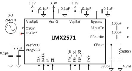 Figure 62. Typical Synthesizer Duplex Mode Application Schematic
8.2.1.1 Design Requirements
OSCin frequency = 26 MHz, LVCMOS
RFoutTx frequency = 902 MHz
RFoutRx frequency = 928 MHz
Frequency switching time ≤ 500 µs
4FSK modulation on TX, baud rate = 20 kSPs
Frequency deviation = ±10 kHz and ±30 kHz
FSK error ≤ 1 %
Spurs ≤ –72 dBc
Lock detect is required to indicate lock status
Output power < 1 dBm
8.2.1.2 Detailed Design Procedure
First of all, calculate all the frequencies in each functional block.
 Figure 63. F1 Frequency Plan
Assign F1 frequency to be 902 MHz. With CHDIV1 = 5 and CHDIV2 = 1, the total division is 5. As a result, the VCO frequency will be 902 * 5 = 4510 MHz, which is within the VCO tuning range.
OSCin is 26 MHz, put Pre-divider = 1 to meet the MULT input frequency range requirement.
To meet the maximum MULT output frequency requirement, possible MULT values are 3 to 5. Play around the allowable MULT values and Post-divider values to get the optimum phase noise and spurs performance. Assuming MULT = 4 and Post-divider = 1 returns the best performance, then fPD = 104 MHz.
N-divider = 21.68269231, that means Ninteger = 21 while Nfrac = 0.68269231. To use the direct digital modulation feature, put fractional denominator, DEN = 0. The actual DEN value is, in fact, equal to 224 = 16777216. So the fractional numerator, NUM, is equal to Nfrac * DEN = 11453676.
Use Equation 4 and Equation 6 to calculate the required FSK steps. For +10 kHz frequency deviation, the FSK step value is equal to [10000 * 16777216 / (104 * 106)] * (5 * 1 / 2) = 4033. For –10 kHz frequency deviation, the FSK step value is equal to 2's complement of 4033 = 61502. Similarly, the FSK step values for ±30 kHz frequency deviation are 12099 and 53436.
All the required configuration values for F2, 928 MHz can be calculated in the similar fashion and are summarized as follows:
Table 41. Frequency Plan Summary
| CONFIGURATION PARAMETER | F1 (902 MHz) | F2 (928 MHz) |
|---|---|---|
| Pre-divider | 1 | 1 |
| MULT | 4 | 4 |
| Post-divider | 1 | 1 |
| 104 MHz | 104 MHz | |
| VCO | 4510 MHz | 4640 MHz |
| N-divider | 21.68269231 | 22.30769231 |
| Ninteger | 21 | 22 |
| DEN | 0 | 0 |
| NUM | 11453676 | 5162220 |
| CHDIV1 | 5 | 5 |
| CHDIV2 | 1 | 1 |
| FSK_DEV0 | 4033 | |
| FSK_DEV1 | 12099 | |
| FSK_DEV2 | 61502 | |
| FSK_DEV3 | 53436 |
Assume here that the base charge pump current = 1250 µA, CP Gain = 1x and 3rd order Delta Sigma Modulator without dithering is adopted in both frequency sets. The register settings are summarized as follows:
Table 42. Register Settings Summary
| CONFIGURATION PARAMETERS | REGISTER BIT | COMMON SETTING | F1 SPECIFIC SETTING | F2 SPECIFIC SETTING |
|---|---|---|---|---|
| VCO calibration | FCAL_EN | 1 = Enabled | ||
| Lock detect | SDO_LE_SEL | 1 = Lock detect output | ||
| LD_EN | 1 = Enabled | |||
| OSCin buffer type | IPBUF_SE_DIFF_SEL | 0 = SE input buffer | ||
| Dithering | DITHERING | 0 = Disabled | ||
| Charge pump gain | CP_GAIN | 1 = 1x | ||
| Base charge pump current | CP_IUP | 8 = 1250 µA | ||
| CP_IDN | 8 = 1250 µA | |||
| MULT settling time | MULT_WAIT | 520 = 20 µs | ||
| Output buffer type | OUTBUF_RX_TYPE | 1 = Push pull | ||
| OUTBUF_TX_TYPE | 1 = Push pull | |||
| Output buffer auto mute | OUTBUF_AUTOMUTE | 0 = Disabled | ||
| TrCtl pin polarity | RXTX_POL | 0 = Active LOW = TX | ||
| TX RX switching mode | RXTX_CTRL | 1 = TrCtl pin control | ||
| Enable F1 F2 initialization | F1F2_MODE | 1 = Enabled | ||
| F1 F2 switching mode | F1F2_CTRL | 1 = Control by TrCtl pin | ||
| Pre-divider | PLL_R_PRE_F1 | 1 | ||
| PLL_R_PRE_F2 | 1 | |||
| MULT multiplier | MULT_F1 | 4 | ||
| MULT_F2 | 4 | |||
| Post-divider | PLL_R_F1 | 1 | ||
| PLL_R_F2 | 1 | |||
| ΔΣ modulator order | FRAC_ORDER_F1 | 3 = 3rd order | ||
| FRAC_ORDER_F2 | 3 = 3rd order | |||
| PFD delay | PFD_DELAY_F1 | 5 = 8 clock cycles | ||
| PFD_DELAY_F2 | 5 = 8 clock cycles | |||
| CHDIV1 divider | CHDIV1_F1 | 1 = Divide by 5 | ||
| CHDIV1_F2 | 1 = Divide by 5 | |||
| CHDIV2 divider | CHDIV2_F1 | 0 = Divide by 1 | ||
| CHDIV2_F2 | 0 = Divide by 1 | |||
| Internal 3rd pole loop filter | LF_R3_F1 | 4 = 800 Ω | ||
| LF_R3_F2 | 4 = 800 Ω | |||
| Internal 4th pole loop filter | LF_R4_F1 | 4 = 800 Ω | ||
| LF_R4_F2 | 4 = 800 Ω | |||
| Output port selection | OUTBUF_TX_EN_F1 | 1 = TX port enabled | ||
| OUTBUF_RX_EN_F2 | 1 = RX port enabled | |||
| Output power control | OUTBUF_TX_PWR_F1 | 6 | ||
| OUTBUF_RX_PWR_F2 | 6 | |||
| FSK mode | FSK_MODE_SEL1 FSK_MODE_SEL0 |
00 = FSK PIN mode | ||
| FSK level | FSK_LEVEL | 2 = 4FSK | ||
| Enable FSK modulation | FSK_EN_F1 | 1 = Enabled | ||
| FSK deviation at 00 | FSK_DEV0_F1 | 4033 = +10 kHz | ||
| FSK deviation at 01 | FSK_DEV1_F1 | 12099 = +30 kHz | ||
| FSK deviation at 10 | FSK_DEV2_F1 | 61502 = -10 kHz | ||
| FSK deviation at 11 | FSK_DEV3_F1 | 53436 = -30 kHz | ||
| Fractional denominator | PLL_DEN_F1[23:16] | 0 | ||
| PLL_DEN_F1[15:0] | 0 | |||
| PLL_DEN_F2[23:16] | 0 | |||
| PLL_DEN_F2[15:0] | 0 | |||
| Fractional numerator | PLL_NUM_F1[23:16] | 174 | ||
| PLL_NUM_F1[15:0] | 50412 | |||
| PLL_NUM_F2[23:16] | 78 | |||
| PLL_NUM_F2[15:0] | 50412 | |||
| Ninteger | PLL_N_F1 | 21 | ||
| PLL_N_F2 | 22 | |||
| Prescaler | PLL_N_PRE_F1 | 0 = Divide by 2 | ||
| PLL_N_PRE_F2 | 0 = Divide by 2 |
8.2.1.3 Synthesizer Duplex Mode Application Curves
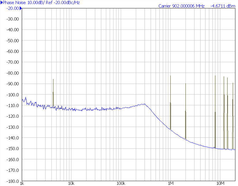 Figure 64. F1 (TX) Phase Noise and Spurs
_SNAS654.png) Figure 66. F1 (TX) to F2 (RX) Switching
Figure 66. F1 (TX) to F2 (RX) Switching
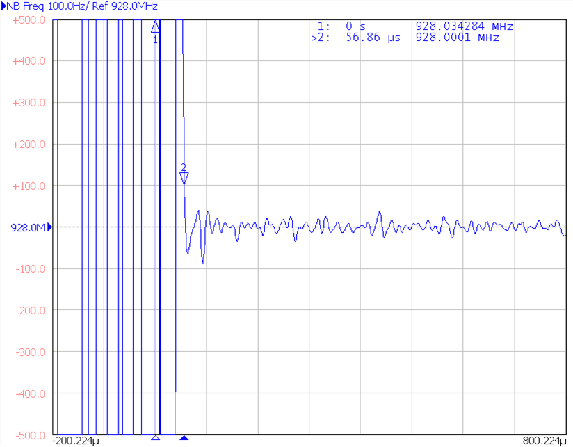 Figure 68. F1 to F2 Switching Time
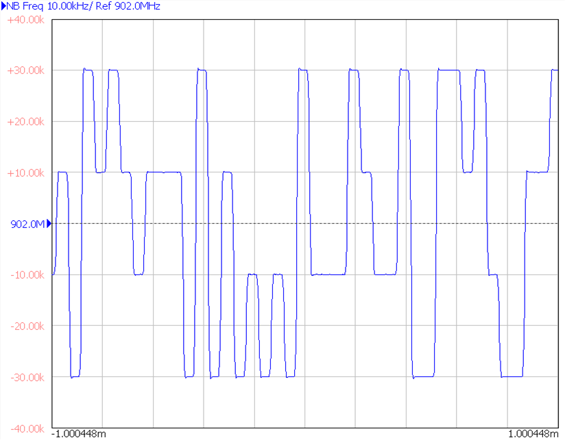 Figure 70. 4FSK Modulation
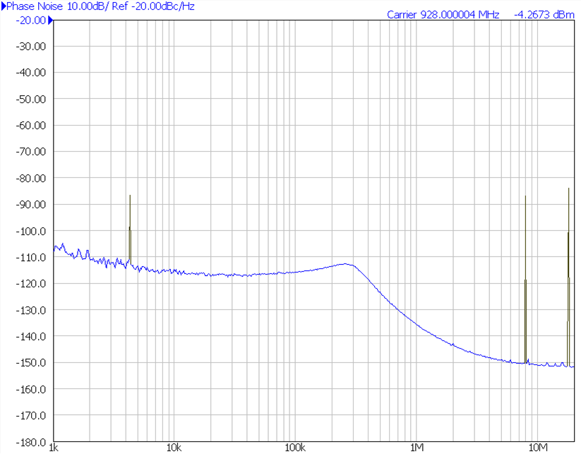 Figure 65. F2 (RX) Phase Noise and Spurs
_SNAS654.png) Figure 67. F2 (RX) to F1 (TX) Switching
Figure 67. F2 (RX) to F1 (TX) Switching
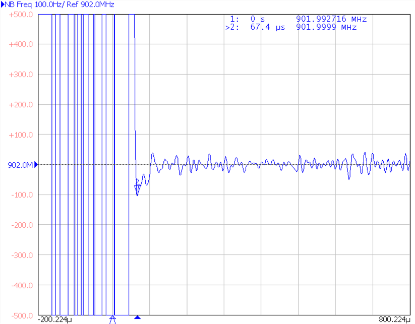 Figure 69. F2 to F1 Switching Time
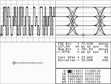 Figure 71. 4FSK Modulation Quality
8.2.2 PLL Duplex Mode
In this example, the internal VCO will be bypassed, and the device is used to lock to an external VCO. TI’s dual SPST analog switch, TS5A21366 is used to facilitate FastLock between two frequencies.
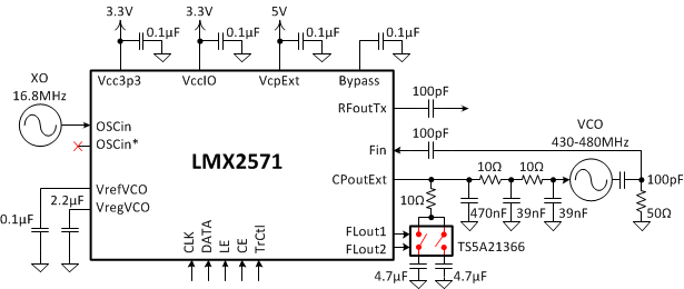 Figure 72. Typical PLL Duplex Mode Application Schematic
8.2.2.1 Design Requirements
OSCin frequency = 16.8 MHz, LVCMOS
F1 frequency = 430 MHz
F2 frequency = 480 MHz
Frequency switching time ≤ 1.5 ms within 100-Hz frequency tolerance
8.2.2.2 Detailed Design Procedure
Again, we need to figure out all the frequencies in each functional block first.
 Figure 73. Frequency Plan in PLL Duplex Mode
Follow the previous example to determine all the necessary configurations. Table 43 is the summary in this example.
Table 43. PLL Duplex Mode Frequency Plan Summary
| CONFIGURATION PARAMETER | F1 (430 MHz) | F2 (480 MHz) |
|---|---|---|
| Pre-divider | 1 | 1 |
| MULT | 5 | 5 |
| Post-divider | 3 | 3 |
| 28 MHz | 28 MHz | |
| VCO | 430 MHz | 480 MHz |
| N-divider | 15.35714286 | 17.14285714 |
| Ninteger | 15 | 17 |
| DEN | 1234567 | 1234567 |
| NUM | 440917 | 176367 |
To enable external VCO operation, set the following bits:
Table 44. PLL Duplex Mode Register Settings Summary
| CONFIGURATION PARAMETER | REGISTER BITS | SETTING |
|---|---|---|
| Charge pump polarity | EXTVCO_CP_POL | 0 = Positive |
| External VCO charge pump gain | EXTVCO_CP_GAIN | 1 = 1x |
| Base charge pump current | EXTVCO_CP_IUP | 8 = 1250 µA |
| EXTVCO_CP_IDN | 8 = 1250 µA | |
| Select PLL mode operation | EXTVCO_SEL_F1, EXTVCO_SEL_F2 | 1 = External VCO |
| CHDIV3 divider | EXTVCO_CHDIV_F1, EXTVCO_CHDIV_F2 | 0 = Bypass |
Make sure that register R0, FCAL_EN is set so that FastLock is enabled.
The loop bandwidth had been design to be around 4 kHz, while phase margin is about 40 degrees.
8.2.2.3 PLL Duplex Mode Application Curves
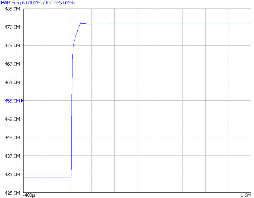 Figure 74. F1 to F2 Switching
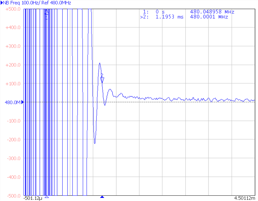 Figure 76. F1 to F2 Switching Time
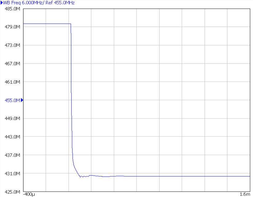 Figure 75. F2 to F1 Switching
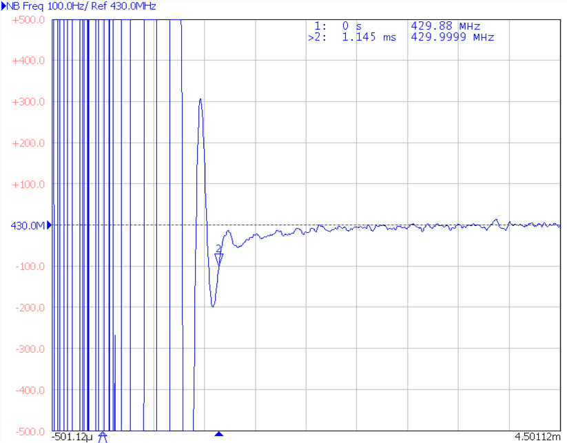 Figure 77. F2 to F1 Switching Time
8.2.3 Synthesizer/PLL Duplex Mode
This example will demonstrate the device's capability in switching two frequencies using internal and external VCO. VCO switching is toggled by the TrCtl pin. Direct digital FSK modulation is enabled in TX using FSK I2S mode.
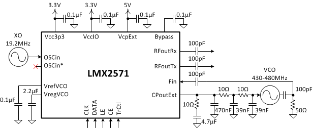 Figure 78. Typical Synthesizer/PLL Duplex Mode Application Schematic
8.2.3.1 Design Requirements
OSCin frequency = 19.2 MHz, LVCMOS
RFoutRX frequency = 440 MHz, external VCO = F1
RFoutTx frequency = 540 MHz, internal VCO = F2
Frequency switching time ≤ 1.5 ms within 100-Hz frequency tolerance
Arbitrary FSK modulation to simulate analog FM modulation (10 times and 20 times over-sampling rate)
FM modulation frequency = 1 kHz
Frequency deviation = ±2000 Hz
Spurs ≤ –72 dBc
8.2.3.2 Detailed Design Procedure
Frequency plans in TX and RX paths are as follows:
 Figure 79. TX and RX Frequency Plans
Follow the previous examples to determine all the necessary configurations. To enable FSK I2S mode, set
FSK_MODE_SEL1=1
FSK_MODE_SEL=0
FSK_EN_F2=1
8.2.3.3 Synthesizer/PLL Duplex Mode Application Curves
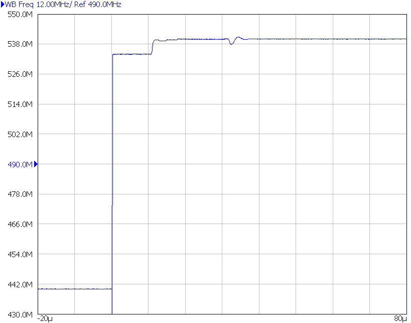 Figure 80. External VCO to Internal VCO Switching
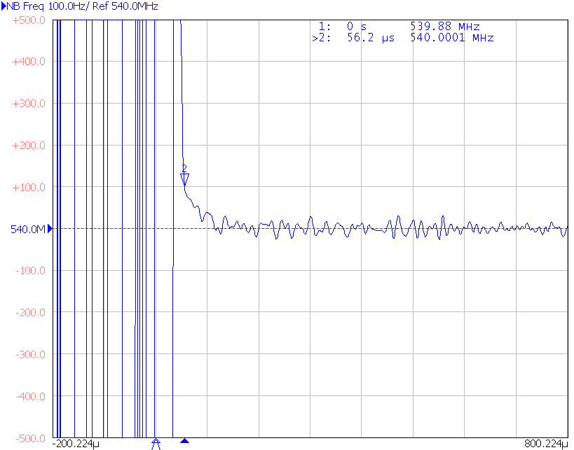 Figure 82. External VCO to Internal VCO Switching Time
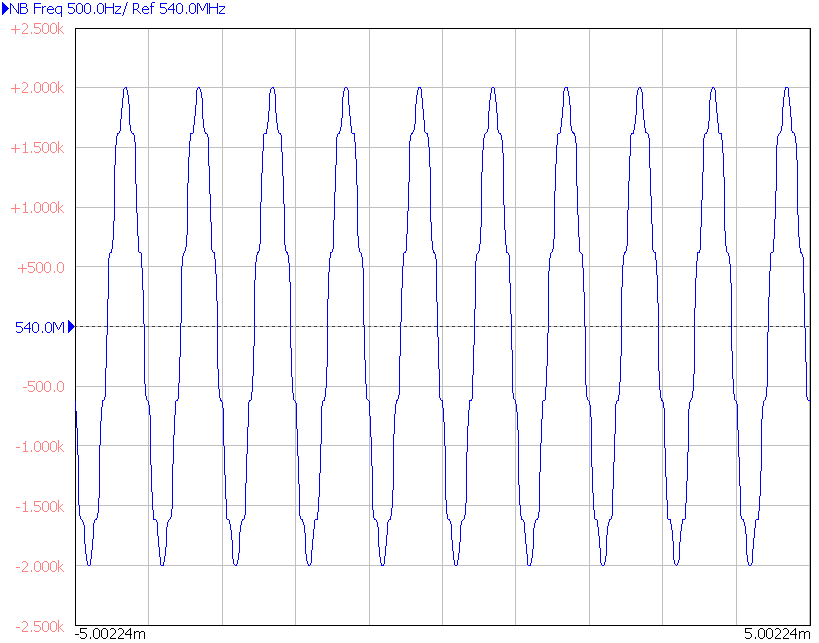 Figure 84. Simulated FM Modulation (10 times over-sampling)
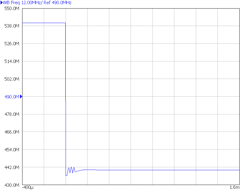 Figure 81. Internal VCO to External VCO Switching
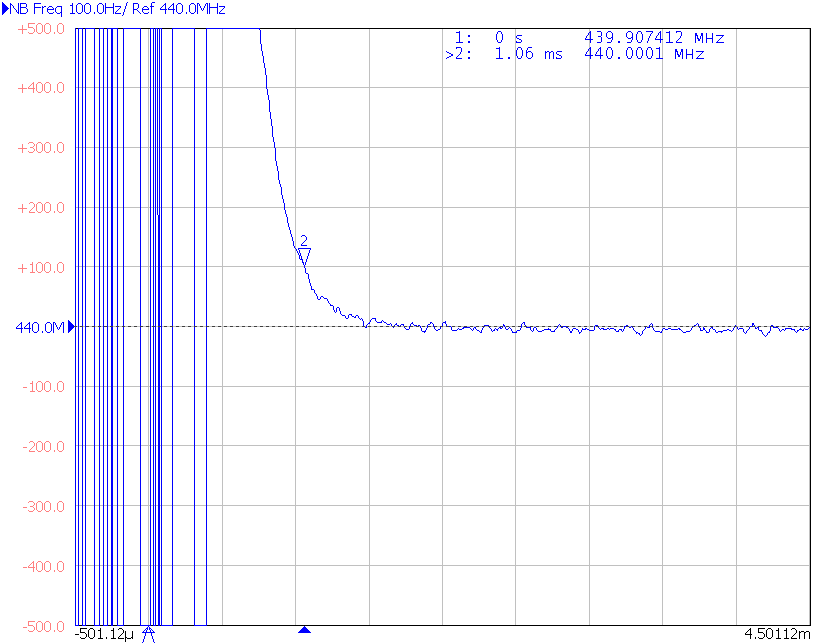 Figure 83. Internal VCO to External VCO Switching Time
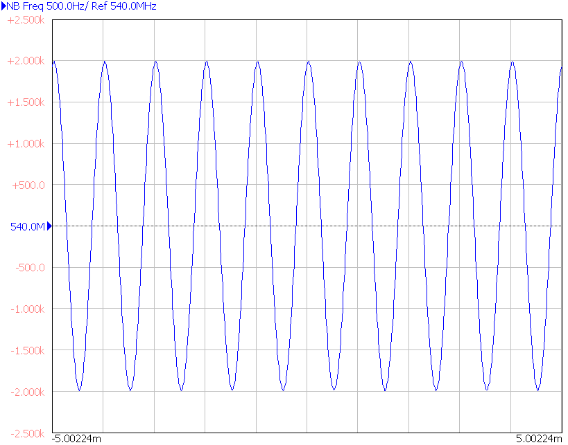 Figure 85. Simulated FM Modulation (20 times over-sampling)
8.3 Do's and Don'ts
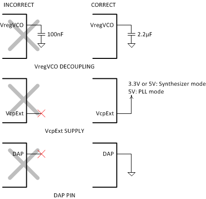 Figure 86. Do's and Don'ts